Home > Press > Berkeley Lab Researchers Ink Nanostructures with Tiny ‘Soldering Iron’
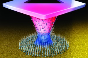 |
| Thermal dip-pen nanolithography turns the tip of a scanning probe microscope into a tiny soldering iron that can be used to draw chemical patterns as small as 20 nanometers on surfaces. (Image courtesy of DeYoreo, et. al) |
Abstract:
Researchers with the U.S. Department of Energy (DOE)'s Lawrence Berkeley National Laboratory (Berkeley Lab) have shed light on the role of temperature in controlling a fabrication technique for drawing chemical patterns as small as 20 nanometers. This technique could provide an inexpensive, fast route to growing and patterning a wide variety of materials on surfaces to build electrical circuits and chemical sensors, or study how pharmaceuticals bind to proteins and viruses.
Berkeley Lab Researchers Ink Nanostructures with Tiny ‘Soldering Iron’
Berkeley, CA | Posted on November 7th, 2011One way of directly writing nanoscale structures onto a substrate is to use an atomic force microscope (AFM) tip as a pen to deposit ink molecules through molecular diffusion onto the surface. Unlike conventional nanofabrication techniques that are expensive, require specialized environments and usually work with only a few materials, this technique, called dip-pen nanolithography, can be used in almost any environment to write many different chemical compounds. A cousin of this technique — called thermal dip-pen nanolithography — extends this technique to solid materials by turning an AFM tip into a tiny soldering iron.
Dip-pen nanolithography can be used to pattern features as small as 20 nanometers, more than forty thousand times smaller than the width of a human hair. What's more, the writing tip also performs as a surface profiler, allowing a freshly-writ surface to be imaged with nanoscale precision immediately after patterning.
"Tip-based manufacturing holds real promise for precise fabrication of nanoscale devices," says Jim DeYoreo, interim director of Berkeley Lab's Molecular Foundry, a DOE nanoscience research center. "However, a robust technology requires a scientific foundation built on an understanding of material transfer during this process. Our study is the first to provide this fundamental understanding of thermal dip-pen nanolithography."
In this study, DeYoreo and coworkers systematically investigated the effect of temperature on feature size. Using their results, the team developed a new model to deconstruct how ink molecules travel from the writing tip to the substrate, assemble into an ordered layer and grow into a nanoscale feature.
"By carefully considering the role of temperature in thermal dip-pen nanolithography, we may be able to design and fabricate nanoscale patterns of materials ranging from small molecules to polymers with better control over feature sizes and shapes on a variety of substrates," says Sungwook Chung, a staff scientist in Berkeley Lab's Physical Biosciences Division, and Foundry user working with DeYoreo. "This technique helps overcome fundamental length scale limitations without the need for complex growth methods."
DeYoreo and Chung collaborated with a research team from the University of Illinois at Urbana-Champaign that specializes in fabricating specialized tips for AFMs. Here, these collaborators developed a silicon-based AFM tip with a gradient of charge-carrying atoms sprinkled into the silicon such that a higher number reside at the base while fewer sit at the tip. This makes the tip heat up when electricity flows through it, much like the burner on an electric stove.
This ‘nanoheater' can then be used to heat up inks applied to the tip, causing them to flow to the surface for fabricating microscale and nanoscale features. The group demonstrated this by drawing dots and lines of the organic molecule mercaptohexadecanoic acid on gold surfaces. The hotter the tip, the larger the feature size the team could draw.
"We are excited about this collaboration with Berkeley Lab, which combines their remarkable nanoscience capabilities with our technology to control temperature and heat flow on the nanometer scale," says co-author William P. King, a University of Illinois professor of mechanical sciences and engineering. "Our ability to control the temperature within a nanometer-scale spot enabled this study of molecular-scale transport. By tuning the hotspot temperature, we can probe how molecules flow to a surface."
"This thermal control over tip-to-surface transfer developed by Professor King's group adds versatility by enabling on-the-fly variations in feature size and patterning of both liquid and solid materials," DeYoreo adds.
Chung is the lead author and DeYoreo the corresponding author of a paper reporting this research in the journal Applied Physics Letters. The paper is titled "Temperature-dependence of ink transport during thermal dip-pen nanolithography." Co-authoring the paper with Chung, DeYoreo and King were Jonathan Felts and Debin Wang.
This work at the Molecular Foundry was supported by DOE's Office of Science and the Defense Advanced Research Projects Agency.
####
About Berkeley Lab
The Molecular Foundry is one of five DOE Nanoscale Science Research Centers (NSRCs), national user facilities for interdisciplinary research at the nanoscale, supported by the DOE Office of Science. Together the NSRCs comprise a suite of complementary facilities that provide researchers with state-of-the-art capabilities to fabricate, process, characterize and model nanoscale materials, and constitute the largest infrastructure investment of the National Nanotechnology Initiative. The NSRCs are located at DOE’s Argonne, Brookhaven, Lawrence Berkeley, Oak Ridge and Sandia and Los Alamos National Laboratories. For more information about the DOE NSRCs, please visit http://science.energy.gov
DOE’s Office of Science is the single largest supporter of basic research in the physical sciences in the United States, and is working to address some of the most pressing challenges of our time. For more information, please visit the Office of Science website at science.energy.gov/
Lawrence Berkeley National Laboratory addresses the world’s most urgent scientific challenges by advancing sustainable energy, protecting human health, creating new materials, and revealing the origin and fate of the universe. Founded in 1931, Berkeley Lab’s scientific expertise has been recognized with 13 Nobel prizes. The University of California manages Berkeley Lab for the U.S. Department of Energy’s Office of Science. For more, visit www.lbl.gov
For more information, please click here
Contacts:
Aditi Risbud
(510)486-4861
Copyright © Berkeley Lab
If you have a comment, please Contact us.Issuers of news releases, not 7th Wave, Inc. or Nanotechnology Now, are solely responsible for the accuracy of the content.
Bookmark:


| Related Links |
![]() For more information about the Molecular Foundry visit the Website at:
For more information about the Molecular Foundry visit the Website at:
| Related News Press |
News and information
![]() Quantum computer improves AI predictions April 17th, 2026
Quantum computer improves AI predictions April 17th, 2026
![]() Flexible sensor gains sensitivity under pressure April 17th, 2026
Flexible sensor gains sensitivity under pressure April 17th, 2026
![]() A reusable chip for particulate matter sensing April 17th, 2026
A reusable chip for particulate matter sensing April 17th, 2026
![]() Detecting vibrational quantum beating in the predissociation dynamics of SF6 using time-resolved photoelectron spectroscopy April 17th, 2026
Detecting vibrational quantum beating in the predissociation dynamics of SF6 using time-resolved photoelectron spectroscopy April 17th, 2026
Laboratories
![]() Researchers develop molecular qubits that communicate at telecom frequencies October 3rd, 2025
Researchers develop molecular qubits that communicate at telecom frequencies October 3rd, 2025
![]() A battery’s hopping ions remember where they’ve been: Seen in atomic detail, the seemingly smooth flow of ions through a battery’s electrolyte is surprisingly complicated February 16th, 2024
A battery’s hopping ions remember where they’ve been: Seen in atomic detail, the seemingly smooth flow of ions through a battery’s electrolyte is surprisingly complicated February 16th, 2024
Govt.-Legislation/Regulation/Funding/Policy
![]() Quantum computer improves AI predictions April 17th, 2026
Quantum computer improves AI predictions April 17th, 2026
![]() Metasurfaces smooth light to boost magnetic sensing precision January 30th, 2026
Metasurfaces smooth light to boost magnetic sensing precision January 30th, 2026
![]() New imaging approach transforms study of bacterial biofilms August 8th, 2025
New imaging approach transforms study of bacterial biofilms August 8th, 2025
Chip Technology
![]() A reusable chip for particulate matter sensing April 17th, 2026
A reusable chip for particulate matter sensing April 17th, 2026
![]() Metasurfaces smooth light to boost magnetic sensing precision January 30th, 2026
Metasurfaces smooth light to boost magnetic sensing precision January 30th, 2026
Nanomedicine
![]() A fundamentally new therapeutic approach to cystic fibrosis: Nanobody repairs cellular defect April 17th, 2026
A fundamentally new therapeutic approach to cystic fibrosis: Nanobody repairs cellular defect April 17th, 2026
![]() New molecular technology targets tumors and simultaneously silences two ‘undruggable’ cancer genes August 8th, 2025
New molecular technology targets tumors and simultaneously silences two ‘undruggable’ cancer genes August 8th, 2025
![]() New imaging approach transforms study of bacterial biofilms August 8th, 2025
New imaging approach transforms study of bacterial biofilms August 8th, 2025
![]() Electrifying results shed light on graphene foam as a potential material for lab grown cartilage June 6th, 2025
Electrifying results shed light on graphene foam as a potential material for lab grown cartilage June 6th, 2025
Sensors
![]() Flexible sensor gains sensitivity under pressure April 17th, 2026
Flexible sensor gains sensitivity under pressure April 17th, 2026
![]() Tiny nanosheets, big leap: A new sensor detects ethanol at ultra-low levels January 30th, 2026
Tiny nanosheets, big leap: A new sensor detects ethanol at ultra-low levels January 30th, 2026
![]() From sensors to smart systems: the rise of AI-driven photonic noses January 30th, 2026
From sensors to smart systems: the rise of AI-driven photonic noses January 30th, 2026
![]() Sensors innovations for smart lithium-based batteries: advancements, opportunities, and potential challenges August 8th, 2025
Sensors innovations for smart lithium-based batteries: advancements, opportunities, and potential challenges August 8th, 2025
Discoveries
![]() Quantum computer improves AI predictions April 17th, 2026
Quantum computer improves AI predictions April 17th, 2026
![]() Flexible sensor gains sensitivity under pressure April 17th, 2026
Flexible sensor gains sensitivity under pressure April 17th, 2026
![]() A reusable chip for particulate matter sensing April 17th, 2026
A reusable chip for particulate matter sensing April 17th, 2026
![]() Detecting vibrational quantum beating in the predissociation dynamics of SF6 using time-resolved photoelectron spectroscopy April 17th, 2026
Detecting vibrational quantum beating in the predissociation dynamics of SF6 using time-resolved photoelectron spectroscopy April 17th, 2026
Announcements
![]() A fundamentally new therapeutic approach to cystic fibrosis: Nanobody repairs cellular defect April 17th, 2026
A fundamentally new therapeutic approach to cystic fibrosis: Nanobody repairs cellular defect April 17th, 2026
![]() UC Irvine physicists discover method to reverse ‘quantum scrambling’ : The work addresses the problem of information loss in quantum computing system April 17th, 2026
UC Irvine physicists discover method to reverse ‘quantum scrambling’ : The work addresses the problem of information loss in quantum computing system April 17th, 2026
Tools
![]() Metasurfaces smooth light to boost magnetic sensing precision January 30th, 2026
Metasurfaces smooth light to boost magnetic sensing precision January 30th, 2026
![]() From sensors to smart systems: the rise of AI-driven photonic noses January 30th, 2026
From sensors to smart systems: the rise of AI-driven photonic noses January 30th, 2026
![]() Japan launches fully domestically produced quantum computer: Expo visitors to experience quantum computing firsthand August 8th, 2025
Japan launches fully domestically produced quantum computer: Expo visitors to experience quantum computing firsthand August 8th, 2025
Printing/Lithography/Inkjet/Inks/Bio-printing/Dyes
![]() Presenting: Ultrasound-based printing of 3D materials—potentially inside the body December 8th, 2023
Presenting: Ultrasound-based printing of 3D materials—potentially inside the body December 8th, 2023
![]() Simple ballpoint pen can write custom LEDs August 11th, 2023
Simple ballpoint pen can write custom LEDs August 11th, 2023
![]() Disposable electronics on a simple sheet of paper October 7th, 2022
Disposable electronics on a simple sheet of paper October 7th, 2022
|
|
||
|
|
||
| The latest news from around the world, FREE | ||
|
|
||
|
|
||
| Premium Products | ||
|
|
||
|
Only the news you want to read!
Learn More |
||
|
|
||
|
Full-service, expert consulting
Learn More |
||
|
|
||