Home > Press > JEOL Opens New Office in Brasil
 |
Abstract:
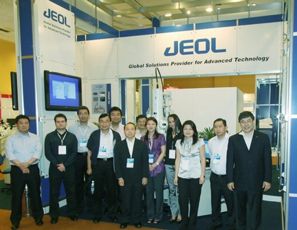
A leading supplier of electron microscopes and scientific instrumentation, JEOL USA (Peabody, Mass.) and its parent company JEOL Ltd. (Akishima, Japan) have opened an office in Sao Paulo, Brasil to support its growing installed base there, and have relocated the personnel to a new facility this month.
JEOL Opens New Office in Brasil
Peabody, MA | Posted on October 3rd, 2011JEOL has enjoyed a 40-year history in Brasil, with the past 30 being through its agent, Fugiwara Enterprises I.C., Ltda. As the number of JEOL customers has continued to grow in the region, the company decided to provide direct support through JEOL service engineers, administrative, and sales personnel.
"We are pleased to be able to provide this focused and complete support to our customer base," said Mr. Hisao Wada, Vice President, JEOL USA and President, JEOL BRASIL Ltda. "We have a long history of working with SEM, TEM, and EPMA users in Brasil and enjoy our relationship with fast-growing industry and academia here."
The new JEOL BRASIL Instrumentos Cientificos Ltda. office is now relocated at Av. Jabaquara, 2958-5oandar-cj.52, 04046-500 Sao Paulo, SP, Brasil (Tel. 55-11-5070-4000).
####
About JEOL
JEOL USA, a wholly-owned subsidiary of JEOL, Ltd., was founded in 1962 in Massachusetts. The U.S. office is also headquarters to JEOL de Mexico, which celebrated its 20th anniversary in 2011, and JEOL Canada, which opened in 1994. In September, JEOL USA entered an agreement with Arquimed, its exclusive agent in Chile.
For more information, please click here
Contacts:
Patricia Corkum
978-536-2273
Copyright © JEOL
If you have a comment, please Contact us.Issuers of news releases, not 7th Wave, Inc. or Nanotechnology Now, are solely responsible for the accuracy of the content.
Bookmark:


| Related News Press |
News and information
![]() Quantum computer improves AI predictions April 17th, 2026
Quantum computer improves AI predictions April 17th, 2026
![]() Flexible sensor gains sensitivity under pressure April 17th, 2026
Flexible sensor gains sensitivity under pressure April 17th, 2026
![]() A reusable chip for particulate matter sensing April 17th, 2026
A reusable chip for particulate matter sensing April 17th, 2026
![]() Detecting vibrational quantum beating in the predissociation dynamics of SF6 using time-resolved photoelectron spectroscopy April 17th, 2026
Detecting vibrational quantum beating in the predissociation dynamics of SF6 using time-resolved photoelectron spectroscopy April 17th, 2026
Imaging
![]() Simple algorithm paired with standard imaging tool could predict failure in lithium metal batteries August 8th, 2025
Simple algorithm paired with standard imaging tool could predict failure in lithium metal batteries August 8th, 2025
Openings/New facilities/Groundbreaking/Expansion
![]() OCSiAl expands its graphene nanotube production capacities to Europe June 17th, 2022
OCSiAl expands its graphene nanotube production capacities to Europe June 17th, 2022
![]() GLOBALFOUNDRIES Moves Corporate Headquarters to its Most Advanced Semiconductor Manufacturing Facility in New York April 27th, 2021
GLOBALFOUNDRIES Moves Corporate Headquarters to its Most Advanced Semiconductor Manufacturing Facility in New York April 27th, 2021
![]() Oxford Instruments Plasma Technology relocates to advanced manufacturing facility: Move driven by exceptional business growth February 12th, 2021
Oxford Instruments Plasma Technology relocates to advanced manufacturing facility: Move driven by exceptional business growth February 12th, 2021
Announcements
![]() A fundamentally new therapeutic approach to cystic fibrosis: Nanobody repairs cellular defect April 17th, 2026
A fundamentally new therapeutic approach to cystic fibrosis: Nanobody repairs cellular defect April 17th, 2026
![]() UC Irvine physicists discover method to reverse �quantum scrambling� : The work addresses the problem of information loss in quantum computing system April 17th, 2026
UC Irvine physicists discover method to reverse �quantum scrambling� : The work addresses the problem of information loss in quantum computing system April 17th, 2026
Tools
![]() Metasurfaces smooth light to boost magnetic sensing precision January 30th, 2026
Metasurfaces smooth light to boost magnetic sensing precision January 30th, 2026
![]() From sensors to smart systems: the rise of AI-driven photonic noses January 30th, 2026
From sensors to smart systems: the rise of AI-driven photonic noses January 30th, 2026
![]() Japan launches fully domestically produced quantum computer: Expo visitors to experience quantum computing firsthand August 8th, 2025
Japan launches fully domestically produced quantum computer: Expo visitors to experience quantum computing firsthand August 8th, 2025
|
|
||
|
|
||
| The latest news from around the world, FREE | ||
|
|
||
|
|
||
| Premium Products | ||
|
|
||
|
Only the news you want to read!
Learn More |
||
|
|
||
|
Full-service, expert consulting
Learn More |
||
|
|
||