Home > Press > NIST Polishes Method for Creating Tiny Diamond Machines
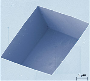 |
| This colorized electron microscope image reveals the boxy shape of the pits the NIST team etched into the diamond surface, exhibiting their smooth vertical sidewalls and flat bottom. The pits were between 1 and 72 micrometers in size.
Credit: NIST |
Abstract:
Diamonds may be best known as a symbol of long-lasting love. But semiconductor makers are also hoping they'll pan out as key components of long-lasting micromachines if a new method developed at the National Institute of Standards and Technology (NIST) for carving these tough, capable crystals proves its worth.* The method offers a precise way to engineer microscopic cuts in a diamond surface, yielding potential benefits in both measurement and technological fields.
NIST Polishes Method for Creating Tiny Diamond Machines
Gaithersburg, MD | Posted on September 30th, 2011By combining their own observations with background gleaned from materials science, NIST semiconductor researchers have found a way to create unique features in diamond�potentially leading to improvements in nanometrology in short order, as it has allowed the team to make holes of precise shape in one of the hardest known substances. But beyond the creation of virtually indestructible nanorulers, the method could one day lead to the improvement of a class of electronic devices useful in cell phones, gyroscopes and medical implants.
Well known for making the hugely complex electronic microchips that run our laptops, the semiconductor industry has expanded its portfolio by fabricating tiny devices with moving parts. Constructed with substantially the same techniques as the electronic chips, these "micro-electromechanical systems," or MEMS, are just a few micrometers in size. They can detect environmental changes such as heat, pressure and acceleration, potentially enabling them to form the basis of tiny sensors and actuators for a host of new devices. But designers must take care that tiny moving parts do not grind to a disastrous halt. One way to make the sliding parts last longer without breaking down is to make them from a tougher material than silicon.
"Diamond may be the ideal substance for MEMS devices," says NIST's Craig McGray. "It can withstand extreme conditions, plus it's able to vibrate at the very high frequencies that new consumer electronics demand. But it's very hard, of course, and there hasn't been a way to engineer it very precisely at small scales. We think our method can accomplish that."
The method uses a chemical etching process to create cavities in the diamond surface. The cubic shape of a diamond crystal can be sliced in several ways�a fact jewelers take advantage of when creating facets on gemstones. The speed of the etching process depends on the orientation of the slice, occurring at a far slower rate in the direction of the cube's "faces"�think of chopping the cube into smaller cubes�and these face planes can be used as a sort of boundary where etching can be made to stop when desired. In their initial experiments, the team created cavities ranging in width from 1 to 72 micrometers, each with smooth vertical sidewalls and a flat bottom.
"We'd like to figure out how to optimize control of this process next," McGray says, "but some of the ways diamond behaved under the conditions we used were unexpected. We plan to explore some of these mysteries while we develop a prototype diamond MEMS device."
* C.D. McGray, R.A. Allen, M. Cangemi and J. Geist. Rectangular scale-similar etch pits in monocrystalline diamond. Diamond and Related Materials. Available online 22 August 2011, ISSN 0925-9635, 10.1016/j.diamond.2011.08.007.
####
For more information, please click here
Contacts:
Chad Boutin
(301) 975-4261
Copyright © NIST
If you have a comment, please Contact us.Issuers of news releases, not 7th Wave, Inc. or Nanotechnology Now, are solely responsible for the accuracy of the content.
Bookmark:


| Related News Press |
News and information
![]() Quantum computer improves AI predictions April 17th, 2026
Quantum computer improves AI predictions April 17th, 2026
![]() Flexible sensor gains sensitivity under pressure April 17th, 2026
Flexible sensor gains sensitivity under pressure April 17th, 2026
![]() A reusable chip for particulate matter sensing April 17th, 2026
A reusable chip for particulate matter sensing April 17th, 2026
![]() Detecting vibrational quantum beating in the predissociation dynamics of SF6 using time-resolved photoelectron spectroscopy April 17th, 2026
Detecting vibrational quantum beating in the predissociation dynamics of SF6 using time-resolved photoelectron spectroscopy April 17th, 2026
Laboratories
![]() Researchers develop molecular qubits that communicate at telecom frequencies October 3rd, 2025
Researchers develop molecular qubits that communicate at telecom frequencies October 3rd, 2025
![]() A battery�s hopping ions remember where they�ve been: Seen in atomic detail, the seemingly smooth flow of ions through a battery�s electrolyte is surprisingly complicated February 16th, 2024
A battery�s hopping ions remember where they�ve been: Seen in atomic detail, the seemingly smooth flow of ions through a battery�s electrolyte is surprisingly complicated February 16th, 2024
Govt.-Legislation/Regulation/Funding/Policy
![]() Quantum computer improves AI predictions April 17th, 2026
Quantum computer improves AI predictions April 17th, 2026
![]() Metasurfaces smooth light to boost magnetic sensing precision January 30th, 2026
Metasurfaces smooth light to boost magnetic sensing precision January 30th, 2026
![]() New imaging approach transforms study of bacterial biofilms August 8th, 2025
New imaging approach transforms study of bacterial biofilms August 8th, 2025
MEMS
Chip Technology
![]() A reusable chip for particulate matter sensing April 17th, 2026
A reusable chip for particulate matter sensing April 17th, 2026
![]() Metasurfaces smooth light to boost magnetic sensing precision January 30th, 2026
Metasurfaces smooth light to boost magnetic sensing precision January 30th, 2026
Nanomedicine
![]() A fundamentally new therapeutic approach to cystic fibrosis: Nanobody repairs cellular defect April 17th, 2026
A fundamentally new therapeutic approach to cystic fibrosis: Nanobody repairs cellular defect April 17th, 2026
![]() New molecular technology targets tumors and simultaneously silences two �undruggable� cancer genes August 8th, 2025
New molecular technology targets tumors and simultaneously silences two �undruggable� cancer genes August 8th, 2025
![]() New imaging approach transforms study of bacterial biofilms August 8th, 2025
New imaging approach transforms study of bacterial biofilms August 8th, 2025
![]() Electrifying results shed light on graphene foam as a potential material for lab grown cartilage June 6th, 2025
Electrifying results shed light on graphene foam as a potential material for lab grown cartilage June 6th, 2025
Sensors
![]() Flexible sensor gains sensitivity under pressure April 17th, 2026
Flexible sensor gains sensitivity under pressure April 17th, 2026
![]() Tiny nanosheets, big leap: A new sensor detects ethanol at ultra-low levels January 30th, 2026
Tiny nanosheets, big leap: A new sensor detects ethanol at ultra-low levels January 30th, 2026
![]() From sensors to smart systems: the rise of AI-driven photonic noses January 30th, 2026
From sensors to smart systems: the rise of AI-driven photonic noses January 30th, 2026
![]() Sensors innovations for smart lithium-based batteries: advancements, opportunities, and potential challenges August 8th, 2025
Sensors innovations for smart lithium-based batteries: advancements, opportunities, and potential challenges August 8th, 2025
Discoveries
![]() Quantum computer improves AI predictions April 17th, 2026
Quantum computer improves AI predictions April 17th, 2026
![]() Flexible sensor gains sensitivity under pressure April 17th, 2026
Flexible sensor gains sensitivity under pressure April 17th, 2026
![]() A reusable chip for particulate matter sensing April 17th, 2026
A reusable chip for particulate matter sensing April 17th, 2026
![]() Detecting vibrational quantum beating in the predissociation dynamics of SF6 using time-resolved photoelectron spectroscopy April 17th, 2026
Detecting vibrational quantum beating in the predissociation dynamics of SF6 using time-resolved photoelectron spectroscopy April 17th, 2026
Materials/Metamaterials/Magnetoresistance
![]() First real-time observation of two-dimensional melting process: Researchers at Mainz University unveil new insights into magnetic vortex structures August 8th, 2025
First real-time observation of two-dimensional melting process: Researchers at Mainz University unveil new insights into magnetic vortex structures August 8th, 2025
![]() Researchers unveil a groundbreaking clay-based solution to capture carbon dioxide and combat climate change June 6th, 2025
Researchers unveil a groundbreaking clay-based solution to capture carbon dioxide and combat climate change June 6th, 2025
![]() A 1960s idea inspires NBI researchers to study hitherto inaccessible quantum states June 6th, 2025
A 1960s idea inspires NBI researchers to study hitherto inaccessible quantum states June 6th, 2025
![]() Institute for Nanoscience hosts annual proposal planning meeting May 16th, 2025
Institute for Nanoscience hosts annual proposal planning meeting May 16th, 2025
Announcements
![]() A fundamentally new therapeutic approach to cystic fibrosis: Nanobody repairs cellular defect April 17th, 2026
A fundamentally new therapeutic approach to cystic fibrosis: Nanobody repairs cellular defect April 17th, 2026
![]() UC Irvine physicists discover method to reverse �quantum scrambling� : The work addresses the problem of information loss in quantum computing system April 17th, 2026
UC Irvine physicists discover method to reverse �quantum scrambling� : The work addresses the problem of information loss in quantum computing system April 17th, 2026
|
|
||
|
|
||
| The latest news from around the world, FREE | ||
|
|
||
|
|
||
| Premium Products | ||
|
|
||
|
Only the news you want to read!
Learn More |
||
|
|
||
|
Full-service, expert consulting
Learn More |
||
|
|
||