Home > Press > Graphene walls could make powerful electronics: Rice, Hong Kong Polytechnic physicists calculate 100 trillion could fit on a chip
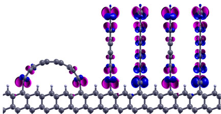 |
| Researchers at Rice University and Hong Kong Polytechnic University calculated that graphene nanoribbons could stand up on diamond or nickel, or even form arches. Up to 100 trillion graphene walls could fit on a square centimeter chip. (Credit: Feng Ding/Hong Kong Polytechnic University) |
Abstract:
To stand a ribbon of graphene upright, it needs diamond on the soles of its shoes.
A new paper by collaborators at Rice University and Hong Kong Polytechnic University demonstrates the possibility that tiny strips of graphene -- one-atom-thick sheets of carbon -- can stand tall on a substrate with a little support. This leads to the possibility that arrays of graphene walls could become ultrahigh density components of electronic or spintronic devices.
Graphene walls could make powerful electronics: Rice, Hong Kong Polytechnic physicists calculate 100 trillion could fit on a chip
Houston, TX | Posted on September 28th, 2011The work was published this month in the online edition of the Journal of the American Chemical Society.
Calculations by Rice theoretical physicist Boris Yakobson, Assistant Professor Feng Ding of Hong Kong Polytechnic and their collaborators showed substrates not only of diamond but also nickel could chemically bind the edge of a strip of a graphene nanoribbon. Because the contact is so slight, the graphene walls retain nearly all of their inherent electrical or magnetic properties.
And because they're so thin, Yakobson and Ding calculated a theoretical potential of putting 100 trillion graphene wall field-effect transistors (FETs) on a square-centimeter chip.
That potential alone may make it possible to blow past the limits implied by Moore's Law -- something Yakobson once discussed with Intel founder Gordon Moore himself.
"We met in Montreal, when nano was a new kid on the block, and had a good conversation," said Yakobson, Rice's Karl F. Hasselmann Chair in Engineering and a professor of materials science and mechanical engineering and of chemistry. "Moore liked to talk about silicon wafers in terms of real estate. Following his metaphor, an upright architecture would increase the density of circuits on a chip -- like going from ranch-style houses in Texas to skyscraper condos in Hong Kong.
"This kind of strategy may help sustain Moore's Law for an extra decade," he said.
A sheet of material a fraction of a nanometer wide is pretty pliable, he said, but the laws of physics are on its side. Binding energies between carbon in the diamond matrix and carbon in graphene are maximized at the edge, and the molecules bind strongly at a 90-degree angle. Minimal energy is required for the graphene to stand upright, which is its preferred state. (Walls on a nickel substrate would be angled at about 30 degrees, the researchers found.)
Yakobson said the walls could be as close to each other as 7/10ths of a nanometer, which would maintain the independent electronic properties of individual nanoribbons. They could potentially be grown on silicon, silicon dioxide, aluminum oxide or silicon carbide.
The research illustrated differences between walls made of two distinct types of graphene, zigzag and armchair, so-called because of the way their edges are shaped.
Sheets of graphene are considered semimetals that have limited use in electronics because electrical current shoots straight through without resistance. However, armchair nanoribbons can become semiconductors; the thinner the ribbon, the larger the band gap, which is essential for transistors.
Zigzag nanoribbons are magnetic. Electrons at their opposing edges spin in opposite directions, a characteristic that can be controlled by an electric current; this makes them suitable for spintronic devices.
In both cases, the electronic properties of the walls can be tuned by changing their height.
The researchers also suggested nanowalls could become nanoarches by attaching opposing ends of a graphene ribbon to the substrate. Rather than lie flat on the diamond or nickel surface, the energies at play along the binding edges would naturally force the graphene strip to rise in the middle. It would essentially become a half-nanotube with its own set of potentially useful properties.
Precisely how to turn these two-dimensional building blocks into a three-dimensional device presents challenges, but the payoff is great, Yakobson said. He noted that the research lays the groundwork for subnanometer electronic technology.
Co-authors of the paper are Qinghong Yuan, Hong Hu and Junfeng Gao of the Institute of Textiles and Clothing, Hong Kong Polytechnic University, and Zhifeng Liu of the Chinese University of Hong Kong. Ding was a research scientist in Yakobson's Rice lab from 2005 to 2009 and has a complimentary appointment at Rice.
####
About Rice University
Located on a 285-acre forested campus in Houston, Texas, Rice University is consistently ranked among the nation's top 20 universities by U.S. News & World Report. Rice has highly respected schools of Architecture, Business, Continuing Studies, Engineering, Humanities, Music, Natural Sciences and Social Sciences and is known for its �unconventional wisdom." With 3,485 undergraduates and 2,275 graduate students, Rice's undergraduate student-to-faculty ratio is less than 6-to-1. Its residential college system builds close-knit communities and lifelong friendships, just one reason why Rice has been ranked No. 1 for best quality of life multiple times by the Princeton Review and No. 4 for "best value" among private universities by Kiplinger's Personal Finance. To read "What they're saying about Rice," go to www.rice.edu/nationalmedia/Rice.pdf.
For more information, please click here
Contacts:
David Ruth
713-348-6327
Mike Williams
713-348-6728
Copyright © Rice University
If you have a comment, please Contact us.Issuers of news releases, not 7th Wave, Inc. or Nanotechnology Now, are solely responsible for the accuracy of the content.
Bookmark:


| Related Links |
![]() View short videos illustrating graphene walls at the American Chemical Society site:
View short videos illustrating graphene walls at the American Chemical Society site:
| Related News Press |
News and information
![]() Quantum computer improves AI predictions April 17th, 2026
Quantum computer improves AI predictions April 17th, 2026
![]() Flexible sensor gains sensitivity under pressure April 17th, 2026
Flexible sensor gains sensitivity under pressure April 17th, 2026
![]() A reusable chip for particulate matter sensing April 17th, 2026
A reusable chip for particulate matter sensing April 17th, 2026
![]() Detecting vibrational quantum beating in the predissociation dynamics of SF6 using time-resolved photoelectron spectroscopy April 17th, 2026
Detecting vibrational quantum beating in the predissociation dynamics of SF6 using time-resolved photoelectron spectroscopy April 17th, 2026
Videos/Movies
![]() ICFO researchers overcome long-standing bottleneck in single photon detection with twisted 2D materials August 8th, 2025
ICFO researchers overcome long-standing bottleneck in single photon detection with twisted 2D materials August 8th, 2025
Graphene/ Graphite
![]() Electrifying results shed light on graphene foam as a potential material for lab grown cartilage June 6th, 2025
Electrifying results shed light on graphene foam as a potential material for lab grown cartilage June 6th, 2025
![]() Breakthrough in proton barrier films using pore-free graphene oxide: Kumamoto University researchers achieve new milestone in advanced coating technologies September 13th, 2024
Breakthrough in proton barrier films using pore-free graphene oxide: Kumamoto University researchers achieve new milestone in advanced coating technologies September 13th, 2024
Chip Technology
![]() A reusable chip for particulate matter sensing April 17th, 2026
A reusable chip for particulate matter sensing April 17th, 2026
![]() Metasurfaces smooth light to boost magnetic sensing precision January 30th, 2026
Metasurfaces smooth light to boost magnetic sensing precision January 30th, 2026
Discoveries
![]() Quantum computer improves AI predictions April 17th, 2026
Quantum computer improves AI predictions April 17th, 2026
![]() Flexible sensor gains sensitivity under pressure April 17th, 2026
Flexible sensor gains sensitivity under pressure April 17th, 2026
![]() A reusable chip for particulate matter sensing April 17th, 2026
A reusable chip for particulate matter sensing April 17th, 2026
![]() Detecting vibrational quantum beating in the predissociation dynamics of SF6 using time-resolved photoelectron spectroscopy April 17th, 2026
Detecting vibrational quantum beating in the predissociation dynamics of SF6 using time-resolved photoelectron spectroscopy April 17th, 2026
Announcements
![]() A fundamentally new therapeutic approach to cystic fibrosis: Nanobody repairs cellular defect April 17th, 2026
A fundamentally new therapeutic approach to cystic fibrosis: Nanobody repairs cellular defect April 17th, 2026
![]() UC Irvine physicists discover method to reverse �quantum scrambling� : The work addresses the problem of information loss in quantum computing system April 17th, 2026
UC Irvine physicists discover method to reverse �quantum scrambling� : The work addresses the problem of information loss in quantum computing system April 17th, 2026
Interviews/Book Reviews/Essays/Reports/Podcasts/Journals/White papers/Posters
![]() A fundamentally new therapeutic approach to cystic fibrosis: Nanobody repairs cellular defect April 17th, 2026
A fundamentally new therapeutic approach to cystic fibrosis: Nanobody repairs cellular defect April 17th, 2026
![]() UC Irvine physicists discover method to reverse �quantum scrambling� : The work addresses the problem of information loss in quantum computing system April 17th, 2026
UC Irvine physicists discover method to reverse �quantum scrambling� : The work addresses the problem of information loss in quantum computing system April 17th, 2026
Research partnerships
![]() Lab to industry: InSe wafer-scale breakthrough for future electronics August 8th, 2025
Lab to industry: InSe wafer-scale breakthrough for future electronics August 8th, 2025
![]() HKU physicists uncover hidden order in the quantum world through deconfined quantum critical points April 25th, 2025
HKU physicists uncover hidden order in the quantum world through deconfined quantum critical points April 25th, 2025
|
|
||
|
|
||
| The latest news from around the world, FREE | ||
|
|
||
|
|
||
| Premium Products | ||
|
|
||
|
Only the news you want to read!
Learn More |
||
|
|
||
|
Full-service, expert consulting
Learn More |
||
|
|
||