Home > Press > Om Nanotech- Shining Star in the Indian IT Industry
 |
Abstract:
Om Nanotech Pvt. Ltd. the leading manufacturer, supplier and exporter of Memory Modules, Computer RAM, Pen Drives, Flash Cards, has been leading in innovation and bringing first-time technologies to India. After successfully establishing DRAM/Flash IC calibration/testing, Om Nanotech Pvt. Ltd. has now ventured into Die Testing for DRAM/Flash, which is again a First in India.
Om Nanotech- Shining Star in the Indian IT Industry
New Delhi, India | Posted on August 2nd, 2011Explaining the die testing facility at Om Nanotech�s manufacturing unit, Mr. Atul Khosla, Director, Om Nanotech Pvt. Ltd. said, "The Die Testing is a complex process which testing the Die before it is converted to an IC. Die is made from Wafers that are manufactured in highly complex FABS. There are only a handful of DRAM/FLASH FABs globally. Wafers are very thin disks of pure silicon on which minute circuits are etched using very nano-meter lasers. The wafer could have hundreds of Dies� (circuits) etched in a single wafer. These wafers normally come in 8", 10" and 12" diameter sizes, which are then cut to produce Die. Die can be perceived as the smallest unit which independently has the complete functionality desired from the IC. This Die is subsequently sent for packaging which involves encapsulating the Die with special plastics (black colored body), after connecting the connector pads on the Die to external terminals using extremely thin gold wires. Die probing requires specialized probes that need handling under a microscope."
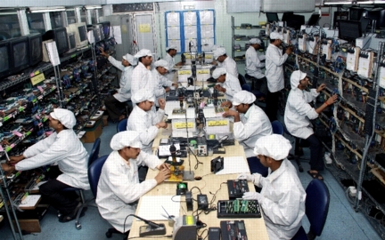
"Along with its contribution in the manufacturing of memory products, we are proud that our manufacturing unit has also resulted as a source of employment for a number of people," added Mr. Khosla.
At the die testing facility, Om Nanotech conducts die probing which ensures that the Die has no inherent problems that may result in low yields after the Die has been packaged into IC . Obviously, the Die that is faulty, results in a faulty packaged IC, leading to wastage of investment on the packaging itself
To master this technology, Om Nanotech Pvt. Ltd. Organized specialized overseas training. The team got extended training and successfully replicated Die Testing at it�s Noida facility, without any further assistance from any external party. Om Nanotech Pvt. Ltd. has currently established a Die Testing capacity of 9 million die per annum.
####
About Om Nanotech Pvt. Ltd.
OM Nanotech Pvt. Ltd. is the largest exporter of memory modules and Flash products, operating from a 24,000 sq. ft. ISO 9000:2008, a state-of-art facility out of NSEZ, Noida. Om Nanotech is probably the First facility in India to undertake DRAM and Flash IC testing and Die testing, With a well-trained manpower of 450 working out of largest-of-its-kind facility in India, Om Nanotech has following production capacities:
Memory Modules: 2.5 million per year
Dram IC Testing: 40 million per year
Flash IC Testing: 9 million per year
Flash Drive : 0.6 million per year
Die Testing: 9 million per year
The manufacturer, Om Nanotech Pvt Ltd., subsidiary of Om Associates Pte Ltd, Singapore, is the recipient of �Best Exporter� award for 2007-08 and 2008 - 09 from Ministry of Commerce. The parent company has also bagged many awards in Singapore like Part of Top 50 Fastest Growing Companies in Singapore - Enterprise 50 (2010), Top Entrepreneur of the Year 2010, Entrepreneur of the Year 2010 (SICCI), Global Trader Award 2009 etc.
For more information, please click here
Contacts:
Alliance Public Relations Pvt. Ltd.
D-1/14,Hauz Khas,
New Delhi-110 016
Tel:
E-Mail:-
www.proalliancepr.com
Copyright © Om Nanotech Pvt. Ltd.
If you have a comment, please Contact us.Issuers of news releases, not 7th Wave, Inc. or Nanotechnology Now, are solely responsible for the accuracy of the content.
Bookmark:


| Related News Press |
News and information
![]() Quantum computer improves AI predictions April 17th, 2026
Quantum computer improves AI predictions April 17th, 2026
![]() Flexible sensor gains sensitivity under pressure April 17th, 2026
Flexible sensor gains sensitivity under pressure April 17th, 2026
![]() A reusable chip for particulate matter sensing April 17th, 2026
A reusable chip for particulate matter sensing April 17th, 2026
![]() Detecting vibrational quantum beating in the predissociation dynamics of SF6 using time-resolved photoelectron spectroscopy April 17th, 2026
Detecting vibrational quantum beating in the predissociation dynamics of SF6 using time-resolved photoelectron spectroscopy April 17th, 2026
Chip Technology
![]() A reusable chip for particulate matter sensing April 17th, 2026
A reusable chip for particulate matter sensing April 17th, 2026
![]() Metasurfaces smooth light to boost magnetic sensing precision January 30th, 2026
Metasurfaces smooth light to boost magnetic sensing precision January 30th, 2026
Memory Technology
![]() Researchers tackle the memory bottleneck stalling quantum computing October 3rd, 2025
Researchers tackle the memory bottleneck stalling quantum computing October 3rd, 2025
![]() First real-time observation of two-dimensional melting process: Researchers at Mainz University unveil new insights into magnetic vortex structures August 8th, 2025
First real-time observation of two-dimensional melting process: Researchers at Mainz University unveil new insights into magnetic vortex structures August 8th, 2025
![]() Utilizing palladium for addressing contact issues of buried oxide thin film transistors April 5th, 2024
Utilizing palladium for addressing contact issues of buried oxide thin film transistors April 5th, 2024
Announcements
![]() A fundamentally new therapeutic approach to cystic fibrosis: Nanobody repairs cellular defect April 17th, 2026
A fundamentally new therapeutic approach to cystic fibrosis: Nanobody repairs cellular defect April 17th, 2026
![]() UC Irvine physicists discover method to reverse �quantum scrambling� : The work addresses the problem of information loss in quantum computing system April 17th, 2026
UC Irvine physicists discover method to reverse �quantum scrambling� : The work addresses the problem of information loss in quantum computing system April 17th, 2026
Photonics/Optics/Lasers
![]() Metasurfaces smooth light to boost magnetic sensing precision January 30th, 2026
Metasurfaces smooth light to boost magnetic sensing precision January 30th, 2026
![]() From sensors to smart systems: the rise of AI-driven photonic noses January 30th, 2026
From sensors to smart systems: the rise of AI-driven photonic noses January 30th, 2026
|
|
||
|
|
||
| The latest news from around the world, FREE | ||
|
|
||
|
|
||
| Premium Products | ||
|
|
||
|
Only the news you want to read!
Learn More |
||
|
|
||
|
Full-service, expert consulting
Learn More |
||
|
|
||