Home > Press > Imec develops procedure for carrier profiling in nanowire-based transistors
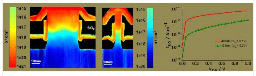 |
| Quantitative 2D-carrier distribution for nanowire diameters of 400nm and 100nm. The difference in drain doping is reflected in the TFET off current. |
Abstract:
Imec's researchers have developed a methodology to quantitatively map the distribution of active dopants in confined 3D-volumes. This is an important step towards in-depth understanding of transistors based on semiconductor nanowires. The new methodology is based on high-vacuum scanning spreading resistance microscopy (HV-SSRM).
Imec develops procedure for carrier profiling in nanowire-based transistors
Leuven, Belgium | Posted on June 16th, 2011Semiconductor nanowires are one of the most promising building blocks for future nanoelectronic devices such as transistors, sensors and solar cells. Nanowire-based tunnel field-effect transistors (TFETs), for example, are widely seen as potential successors of standard MOSFETs, due to the absence of a 60mV/dec sub-threshold swing limitation and reduced short-channel effects.
But to optimize the fabrication processes for such high-performance devices, it is necessary to have a thorough understanding of the active dopant (carrier) distribution. Therefore, researchers from imec have recently extended the applicability of HV-SSRM as a metrology tool for carrier mapping to fully integrated nanowire-based transistors.
Applying HV-SSRM to Si-nanowire-based tunnel-FETs, the team identified a diameter-dependent dopant-deactivation mechanism. This mechanism occurs in small 3D structures only and cannot be predicted using standard process simulation tools. It could be shown experimentally and through device simulations that this phenomenon directly impacts the device characteristics. The validity of the technique is proved by the observance of the diameter dependency of the carrier distribution in the nanowire top-section. This results from a tilted ion implantation step and is perfectly in agreement with results from process simulations.
Scanning spreading resistance microscopy (SSRM) is a technique with a unique combination of high spatial resolution (1 to 3nm) and high sensitivity. SSRM is based on atomic force microscopy and was invented by W. Vandervorst et al. at imec in 1994. During the last decade, it has evolved into the method of choice for carrier profiling in planar MOS transistors. With this work, imec applied HV-SSRM to Si-nanowire-based tunnel-FETs, proving its validity to study carrier distribution in semiconductor nanowires. It also showed that HV-SSRM is capable of revealing physical phenomena which are present in small, 3D structures only, and which cannot be predicted by blanket experiments. Such information is essential for the process development of future nanowire-based devices.
This study has been published in Nanotechnology - issue 18 (volume 22). An illustration from the study was selected for the cover of the journal.
The paper can be accessed on iopscience.iop.org/0957-4484/22/18/185701.
####
About Imec
Imec performs world-leading research in nano-electronics and nano-technology. Its staff of more than 1,900 people includes over 500 industrial residents and guest researchers. Imec�s research is applied in better healthcare, smart electronics, sustainable energy, and safer transport.
For more information, please click here
Contacts:
Barbara Kalkis
Maestro Marketing & PR
Copyright © Imec
If you have a comment, please Contact us.Issuers of news releases, not 7th Wave, Inc. or Nanotechnology Now, are solely responsible for the accuracy of the content.
Bookmark:


| Related News Press |
News and information
![]() Quantum computer improves AI predictions April 17th, 2026
Quantum computer improves AI predictions April 17th, 2026
![]() Flexible sensor gains sensitivity under pressure April 17th, 2026
Flexible sensor gains sensitivity under pressure April 17th, 2026
![]() A reusable chip for particulate matter sensing April 17th, 2026
A reusable chip for particulate matter sensing April 17th, 2026
![]() Detecting vibrational quantum beating in the predissociation dynamics of SF6 using time-resolved photoelectron spectroscopy April 17th, 2026
Detecting vibrational quantum beating in the predissociation dynamics of SF6 using time-resolved photoelectron spectroscopy April 17th, 2026
Possible Futures
![]() A fundamentally new therapeutic approach to cystic fibrosis: Nanobody repairs cellular defect April 17th, 2026
A fundamentally new therapeutic approach to cystic fibrosis: Nanobody repairs cellular defect April 17th, 2026
![]() UC Irvine physicists discover method to reverse �quantum scrambling� : The work addresses the problem of information loss in quantum computing system April 17th, 2026
UC Irvine physicists discover method to reverse �quantum scrambling� : The work addresses the problem of information loss in quantum computing system April 17th, 2026
Sensors
![]() Flexible sensor gains sensitivity under pressure April 17th, 2026
Flexible sensor gains sensitivity under pressure April 17th, 2026
![]() Tiny nanosheets, big leap: A new sensor detects ethanol at ultra-low levels January 30th, 2026
Tiny nanosheets, big leap: A new sensor detects ethanol at ultra-low levels January 30th, 2026
![]() From sensors to smart systems: the rise of AI-driven photonic noses January 30th, 2026
From sensors to smart systems: the rise of AI-driven photonic noses January 30th, 2026
![]() Sensors innovations for smart lithium-based batteries: advancements, opportunities, and potential challenges August 8th, 2025
Sensors innovations for smart lithium-based batteries: advancements, opportunities, and potential challenges August 8th, 2025
Nanoelectronics
![]() Lab to industry: InSe wafer-scale breakthrough for future electronics August 8th, 2025
Lab to industry: InSe wafer-scale breakthrough for future electronics August 8th, 2025
![]() Interdisciplinary: Rice team tackles the future of semiconductors Multiferroics could be the key to ultralow-energy computing October 6th, 2023
Interdisciplinary: Rice team tackles the future of semiconductors Multiferroics could be the key to ultralow-energy computing October 6th, 2023
![]() Key element for a scalable quantum computer: Physicists from Forschungszentrum J�lich and RWTH Aachen University demonstrate electron transport on a quantum chip September 23rd, 2022
Key element for a scalable quantum computer: Physicists from Forschungszentrum J�lich and RWTH Aachen University demonstrate electron transport on a quantum chip September 23rd, 2022
![]() Reduced power consumption in semiconductor devices September 23rd, 2022
Reduced power consumption in semiconductor devices September 23rd, 2022
Announcements
![]() A fundamentally new therapeutic approach to cystic fibrosis: Nanobody repairs cellular defect April 17th, 2026
A fundamentally new therapeutic approach to cystic fibrosis: Nanobody repairs cellular defect April 17th, 2026
![]() UC Irvine physicists discover method to reverse �quantum scrambling� : The work addresses the problem of information loss in quantum computing system April 17th, 2026
UC Irvine physicists discover method to reverse �quantum scrambling� : The work addresses the problem of information loss in quantum computing system April 17th, 2026
Tools
![]() Metasurfaces smooth light to boost magnetic sensing precision January 30th, 2026
Metasurfaces smooth light to boost magnetic sensing precision January 30th, 2026
![]() From sensors to smart systems: the rise of AI-driven photonic noses January 30th, 2026
From sensors to smart systems: the rise of AI-driven photonic noses January 30th, 2026
![]() Japan launches fully domestically produced quantum computer: Expo visitors to experience quantum computing firsthand August 8th, 2025
Japan launches fully domestically produced quantum computer: Expo visitors to experience quantum computing firsthand August 8th, 2025
Solar/Photovoltaic
![]() Spinel-type sulfide semiconductors to operate the next-generation LEDs and solar cells For solar-cell absorbers and green-LED source October 3rd, 2025
Spinel-type sulfide semiconductors to operate the next-generation LEDs and solar cells For solar-cell absorbers and green-LED source October 3rd, 2025
![]() KAIST researchers introduce new and improved, next-generation perovskite solar cell November 8th, 2024
KAIST researchers introduce new and improved, next-generation perovskite solar cell November 8th, 2024
![]() Groundbreaking precision in single-molecule optoelectronics August 16th, 2024
Groundbreaking precision in single-molecule optoelectronics August 16th, 2024
![]() Development of zinc oxide nanopagoda array photoelectrode: photoelectrochemical water-splitting hydrogen production January 12th, 2024
Development of zinc oxide nanopagoda array photoelectrode: photoelectrochemical water-splitting hydrogen production January 12th, 2024
|
|
||
|
|
||
| The latest news from around the world, FREE | ||
|
|
||
|
|
||
| Premium Products | ||
|
|
||
|
Only the news you want to read!
Learn More |
||
|
|
||
|
Full-service, expert consulting
Learn More |
||
|
|
||