Home > Press > FEI Announces New Vion PFIB System for Advanced IC Packaging: Faster Material Removal Opens New Markets for Failure Analysis in Advanced Integrated Circuit Packaging Applications
 |
Abstract:
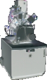
FEI (NASDAQ: FEIC), a leading instrumentation company providing microscopy systems for research and industry, today released the Vion™ plasma focused ion beam (PFIB) system that removes material more than 20 times faster than existing FIB technologies.
FEI Announces New Vion PFIB System for Advanced IC Packaging: Faster Material Removal Opens New Markets for Failure Analysis in Advanced Integrated Circuit Packaging Applications
Hillsboro, OR | Posted on June 13th, 2011Faster (20-50x) material removal addresses new markets for FIB-based failure analysis in advanced integrated circuit (IC) packaging applications that use larger scale structures to connect multiple chips in tightly integrated packages. The Vion PFIB system's ability to provide site-specific cross-sectional analysis of these new technologies in minutes rather than hours will accelerate process development and reduce time-to-market for new products.
"The new Vion PFIB is the first FEI product to incorporate plasma source technology," said Rudy Kellner, vice president and general manager for FEI's Electronics Division. "With more than a microamp of beam current, it can remove material much faster than liquid metal ion sources that typically max out at a few tens of nanoamps, while still preserving excellent milling precision and imaging resolution at low beam currents. The improvement of more than 20x in speed makes it practical to cross section and analyze critical new technologies that have become primary drivers of new product development in the semiconductor industry, such as 3D packaging and 3D transistor design technologies."
According to Dr. Peter Ramm, head of the department for device and 3D integration, Fraunhofer EMFT in Munich, "The increased milling speed provided by FEI's Vion PFIB system lets us perform analysis in minutes, as opposed to several hours on a conventional FIB. This capability is essential for failure analysis of advanced 3D-integrated systems in production, and FEI is releasing the Vion system at just the time when the market needs it."
By combining high-speed milling and deposition with precise control and high-quality imaging, the Vion PFIB system can be used in a variety of critical applications, such as: failure analysis of bumps, wire bonds, through silicon vias (TSVs), and stacked die; site specific removal of package and other materials to enable failure analysis and fault isolation on buried die; circuit and package modifications to test design changes without repeating the fabrication process or creating new masks; process monitoring and development at the package level; and defect analysis of packaged parts and MEMS devices.
Kellner adds, "The electronics industry is an obvious first use case for the new Vion PFIB system, however, we see potential applications in materials science and natural resources as well."
While the plasma source of the Vion PFIB system can deliver more than a microamp of current in a well-focused beam, it can still maintain excellent performance at lower currents used for high-precision final cuts and high-resolution (sub-30 nm) imaging. In addition, by introducing various gases, the Vion PFIB system can selectively etch specific materials or deposit patterned conductors and insulators. The plasma source also offers the potential to use different ion species to enhance performance in specific applications.
The Vion PFIB system is available for ordering immediately.
####
About FEI Company
FEI (Nasdaq: FEIC) is a leading diversified scientific instruments company. It is a premier provider of electron- and ion-beam microscopes and tools for nanoscale applications across many industries: industrial and academic materials research, life sciences, semiconductors, data storage, natural resources and more. With more than 60 years of technological innovation and leadership, FEI has set the performance standard in transmission electron microscopes (TEM), scanning electron microscopes (SEM) and DualBeams™, which combine a SEM with a focused ion beam (FIB). FEI’s imaging systems provide 3D characterization, analysis and modification/prototyping with resolutions down to the sub-Ĺngström (one-tenth of a nanometer) level. FEI’s NanoPorts in North America, Europe and Asia provide centers of technical excellence where its world-class community of customers and specialists collaborate. FEI has approximately 1800 employees and sales and service operations in more than 50 countries around the world.
FEI Safe Harbor Statement
This news release contains forward-looking statements that include statements regarding the performance capabilities and benefits of the Vion PFIB. Factors that could affect these forward-looking statements include but are not limited to failure of the product or technology to perform as expected and achieve anticipated results, unexpected technology problems and challenges, changes to the technology, the inability of FEI, its suppliers or project partners to make the technological advances required for the technology to achieve anticipated results, the inability of customers to develop and deploy the expected new applications and our ability to manufacture, ship and deliver the tools or software as expected. Please also refer to our Form 10-K, Forms 10-Q, Forms 8-K and other filings with the U.S. Securities and Exchange Commission for additional information on these factors and other factors that could cause actual results to differ materially from the forward-looking statements. FEI assumes no duty to update forward-looking statements.
For more information, please click here
Contacts:
Sandy Fewkes
Principal
(media contact)
MindWrite Communications, Inc
+1 408 224 4024
FEI Company
Fletcher Chamberlin
(investors and analysts)
Investor Relations
+1 503 726 7710
Copyright © FEI
If you have a comment, please Contact us.Issuers of news releases, not 7th Wave, Inc. or Nanotechnology Now, are solely responsible for the accuracy of the content.
Bookmark:


| Related News Press |
News and information
![]() Quantum computer improves AI predictions April 17th, 2026
Quantum computer improves AI predictions April 17th, 2026
![]() Flexible sensor gains sensitivity under pressure April 17th, 2026
Flexible sensor gains sensitivity under pressure April 17th, 2026
![]() A reusable chip for particulate matter sensing April 17th, 2026
A reusable chip for particulate matter sensing April 17th, 2026
![]() Detecting vibrational quantum beating in the predissociation dynamics of SF6 using time-resolved photoelectron spectroscopy April 17th, 2026
Detecting vibrational quantum beating in the predissociation dynamics of SF6 using time-resolved photoelectron spectroscopy April 17th, 2026
Chip Technology
![]() A reusable chip for particulate matter sensing April 17th, 2026
A reusable chip for particulate matter sensing April 17th, 2026
![]() Metasurfaces smooth light to boost magnetic sensing precision January 30th, 2026
Metasurfaces smooth light to boost magnetic sensing precision January 30th, 2026
Announcements
![]() A fundamentally new therapeutic approach to cystic fibrosis: Nanobody repairs cellular defect April 17th, 2026
A fundamentally new therapeutic approach to cystic fibrosis: Nanobody repairs cellular defect April 17th, 2026
![]() UC Irvine physicists discover method to reverse ‘quantum scrambling’ : The work addresses the problem of information loss in quantum computing system April 17th, 2026
UC Irvine physicists discover method to reverse ‘quantum scrambling’ : The work addresses the problem of information loss in quantum computing system April 17th, 2026
Tools
![]() Metasurfaces smooth light to boost magnetic sensing precision January 30th, 2026
Metasurfaces smooth light to boost magnetic sensing precision January 30th, 2026
![]() From sensors to smart systems: the rise of AI-driven photonic noses January 30th, 2026
From sensors to smart systems: the rise of AI-driven photonic noses January 30th, 2026
![]() Japan launches fully domestically produced quantum computer: Expo visitors to experience quantum computing firsthand August 8th, 2025
Japan launches fully domestically produced quantum computer: Expo visitors to experience quantum computing firsthand August 8th, 2025
|
|
||
|
|
||
| The latest news from around the world, FREE | ||
|
|
||
|
|
||
| Premium Products | ||
|
|
||
|
Only the news you want to read!
Learn More |
||
|
|
||
|
Full-service, expert consulting
Learn More |
||
|
|
||