Home > Press > Stamping Out Low Cost Nanodevices
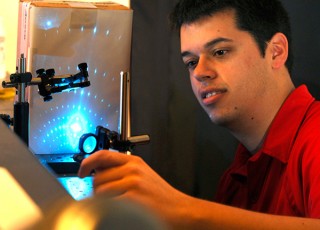 |
| Anne Raynor, Vanderbilt University
Vanderbilt graduate student Jason Ryckman demonstrates operation of a biosensor made from nanoporous materials. |
Abstract:
A simple technique for stamping patterns invisible to the human eye onto a special class of nanomaterials provides a new, cost-effective way to produce novel devices in areas ranging from drug delivery to solar cells.
Stamping Out Low Cost Nanodevices
Nashville, TN | Posted on June 1st, 2011The technique was developed by Vanderbilt University engineers and described in the cover article of the May issue of the journal Nano Letters.
The new method works with materials that are riddled with tiny voids that give them unique optical, electrical, chemical and mechanical properties. Imagine a stiff, sponge-like material filled with holes that are too small to see without a special microscope.
For a number of years, scientists have been investigating the use of these materials - called porous nanomaterials - for a wide range of applications including drug delivery, chemical and biological sensors, solar cells and battery electrodes. There are nanoporous forms of gold, silicon, alumina, and titanium oxide, among others.
Simple stamping
A major obstacle to using the materials has been the complexity and expense of the processing required to make them into devices.
Now, Associate Professor of Electrical Engineering Sharon M. Weiss and her colleagues have developed a rapid, low-cost imprinting process that can stamp out a variety of nanodevices from these intriguing materials.
"It's amazing how easy it is. We made our first imprint using a regular tabletop vise," Weiss said. "And the resolution is surprisingly good."
The traditional strategies used for making devices out of nanoporous materials are based on the process used to make computer chips. This must be done in a special clean room and involves painting the surface with a special material called a resist, exposing it to ultraviolet light or scanning the surface with an electron beam to create the desired pattern and then applying a series of chemical treatments to either engrave the surface or lay down new material. The more complicated the pattern, the longer it takes to make.
About two years ago, Weiss got the idea of creating pre-mastered stamps using the complex process and then using the stamps to create the devices. Weiss calls the new approach direct imprinting of porous substrates (DIPS). DIPS can create a device in less than a minute, regardless of its complexity. So far, her group reports that it has used master stamps more than 20 times without any signs of deterioration.
Process can produce nanoscale patterns
The smallest pattern that Weiss and her colleagues have made to date has features of only a few tens of nanometers, which is about the size of a single fatty acid molecule. They have also succeeded in imprinting the smallest pattern yet reported in nanoporous gold, one with 70-nanometer features.
The first device the group made is a "diffraction-based" biosensor that can be configured to identify a variety of different organic molecules, including DNA, proteins and viruses. The device consists of a grating made from porous silicon treated so that a target molecule will stick to it. The sensor is exposed to a liquid that may contain the target molecule and then is rinsed off. If the target was present, then some of the molecules stick in the grating and alter the pattern of reflected light produced when the grating is illuminated with a laser.
According to the researchers' analysis, when such a biosensor is made from nanoporous silicon it is more sensitive than those made from ordinary silicon.
The Weiss group collaborated with colleagues in Chemical and Biomolecular Engineering to use the new technique to make nano-patterned chemical sensors that are ten times more sensitive than another type of commercial chemical sensor called Klarite that is the basis of a multimillion-dollar market.
The researchers have also demonstrated that they can use the stamps to make precisely shaped microparticles by a process called "over-stamping" that essentially cuts through the nanoporous layer to free the particles from the substrate. One possible application for microparticles made this way from nanoporous silicon are as anodes in lithium-ion batteries, which could significantly increase their capacity without adding a lot of weight.
Vanderbilt University has applied for a patent on the DIPS method.
Vanderbilt graduate student Judson D. Ryckman, Marco Liscidini, University of Pavia and John E. Sipe, University of Toronto, contributed to the research, which was supported by grants from the U.S. Army Research Office, INNESCO project, The National Sciences and Engineering Research Council of Canada and a Graduate Research Fellowship from the National Science Foundation.
Visit Research News @ Vanderbilt for more research news from Vanderbilt.
####
For more information, please click here
Contacts:
David F. Salisbury
(615) 322-NEWS
Copyright © Newswise
If you have a comment, please Contact us.Issuers of news releases, not 7th Wave, Inc. or Nanotechnology Now, are solely responsible for the accuracy of the content.
Bookmark:


| Related News Press |
News and information
![]() Quantum computer improves AI predictions April 17th, 2026
Quantum computer improves AI predictions April 17th, 2026
![]() Flexible sensor gains sensitivity under pressure April 17th, 2026
Flexible sensor gains sensitivity under pressure April 17th, 2026
![]() A reusable chip for particulate matter sensing April 17th, 2026
A reusable chip for particulate matter sensing April 17th, 2026
![]() Detecting vibrational quantum beating in the predissociation dynamics of SF6 using time-resolved photoelectron spectroscopy April 17th, 2026
Detecting vibrational quantum beating in the predissociation dynamics of SF6 using time-resolved photoelectron spectroscopy April 17th, 2026
Chemistry
![]() Projecting light to dispense liquids: A new route to ultra-precise microdroplets January 30th, 2026
Projecting light to dispense liquids: A new route to ultra-precise microdroplets January 30th, 2026
![]() From sensors to smart systems: the rise of AI-driven photonic noses January 30th, 2026
From sensors to smart systems: the rise of AI-driven photonic noses January 30th, 2026
![]() "Nanoreactor" cage uses visible light for catalytic and ultra-selective cross-cycloadditions October 3rd, 2025
"Nanoreactor" cage uses visible light for catalytic and ultra-selective cross-cycloadditions October 3rd, 2025
![]() Cambridge chemists discover simple way to build bigger molecules � one carbon at a time June 6th, 2025
Cambridge chemists discover simple way to build bigger molecules � one carbon at a time June 6th, 2025
Govt.-Legislation/Regulation/Funding/Policy
![]() Quantum computer improves AI predictions April 17th, 2026
Quantum computer improves AI predictions April 17th, 2026
![]() Metasurfaces smooth light to boost magnetic sensing precision January 30th, 2026
Metasurfaces smooth light to boost magnetic sensing precision January 30th, 2026
![]() New imaging approach transforms study of bacterial biofilms August 8th, 2025
New imaging approach transforms study of bacterial biofilms August 8th, 2025
Nanomedicine
![]() A fundamentally new therapeutic approach to cystic fibrosis: Nanobody repairs cellular defect April 17th, 2026
A fundamentally new therapeutic approach to cystic fibrosis: Nanobody repairs cellular defect April 17th, 2026
![]() New molecular technology targets tumors and simultaneously silences two �undruggable� cancer genes August 8th, 2025
New molecular technology targets tumors and simultaneously silences two �undruggable� cancer genes August 8th, 2025
![]() New imaging approach transforms study of bacterial biofilms August 8th, 2025
New imaging approach transforms study of bacterial biofilms August 8th, 2025
![]() Electrifying results shed light on graphene foam as a potential material for lab grown cartilage June 6th, 2025
Electrifying results shed light on graphene foam as a potential material for lab grown cartilage June 6th, 2025
Sensors
![]() Flexible sensor gains sensitivity under pressure April 17th, 2026
Flexible sensor gains sensitivity under pressure April 17th, 2026
![]() Tiny nanosheets, big leap: A new sensor detects ethanol at ultra-low levels January 30th, 2026
Tiny nanosheets, big leap: A new sensor detects ethanol at ultra-low levels January 30th, 2026
![]() From sensors to smart systems: the rise of AI-driven photonic noses January 30th, 2026
From sensors to smart systems: the rise of AI-driven photonic noses January 30th, 2026
![]() Sensors innovations for smart lithium-based batteries: advancements, opportunities, and potential challenges August 8th, 2025
Sensors innovations for smart lithium-based batteries: advancements, opportunities, and potential challenges August 8th, 2025
Discoveries
![]() Quantum computer improves AI predictions April 17th, 2026
Quantum computer improves AI predictions April 17th, 2026
![]() Flexible sensor gains sensitivity under pressure April 17th, 2026
Flexible sensor gains sensitivity under pressure April 17th, 2026
![]() A reusable chip for particulate matter sensing April 17th, 2026
A reusable chip for particulate matter sensing April 17th, 2026
![]() Detecting vibrational quantum beating in the predissociation dynamics of SF6 using time-resolved photoelectron spectroscopy April 17th, 2026
Detecting vibrational quantum beating in the predissociation dynamics of SF6 using time-resolved photoelectron spectroscopy April 17th, 2026
Announcements
![]() A fundamentally new therapeutic approach to cystic fibrosis: Nanobody repairs cellular defect April 17th, 2026
A fundamentally new therapeutic approach to cystic fibrosis: Nanobody repairs cellular defect April 17th, 2026
![]() UC Irvine physicists discover method to reverse �quantum scrambling� : The work addresses the problem of information loss in quantum computing system April 17th, 2026
UC Irvine physicists discover method to reverse �quantum scrambling� : The work addresses the problem of information loss in quantum computing system April 17th, 2026
Military
![]() Quantum engineers �squeeze� laser frequency combs to make more sensitive gas sensors January 17th, 2025
Quantum engineers �squeeze� laser frequency combs to make more sensitive gas sensors January 17th, 2025
![]() Chainmail-like material could be the future of armor: First 2D mechanically interlocked polymer exhibits exceptional flexibility and strength January 17th, 2025
Chainmail-like material could be the future of armor: First 2D mechanically interlocked polymer exhibits exceptional flexibility and strength January 17th, 2025
![]() Single atoms show their true color July 5th, 2024
Single atoms show their true color July 5th, 2024
![]() NRL charters Navy�s quantum inertial navigation path to reduce drift April 5th, 2024
NRL charters Navy�s quantum inertial navigation path to reduce drift April 5th, 2024
Energy
![]() Sensors innovations for smart lithium-based batteries: advancements, opportunities, and potential challenges August 8th, 2025
Sensors innovations for smart lithium-based batteries: advancements, opportunities, and potential challenges August 8th, 2025
![]() Simple algorithm paired with standard imaging tool could predict failure in lithium metal batteries August 8th, 2025
Simple algorithm paired with standard imaging tool could predict failure in lithium metal batteries August 8th, 2025
Battery Technology/Capacitors/Generators/Piezoelectrics/Thermoelectrics/Energy storage
![]() Decoding hydrogen‑bond network of electrolyte for cryogenic durable aqueous zinc‑ion batteries January 30th, 2026
Decoding hydrogen‑bond network of electrolyte for cryogenic durable aqueous zinc‑ion batteries January 30th, 2026
![]() COF scaffold membrane with gate‑lane nanostructure for efficient Li+/Mg2+ separation January 30th, 2026
COF scaffold membrane with gate‑lane nanostructure for efficient Li+/Mg2+ separation January 30th, 2026
![]() MXene nanomaterials enter a new dimension Multilayer nanomaterial: MXene flakes created at Drexel University show new promise as 1D scrolls January 30th, 2026
MXene nanomaterials enter a new dimension Multilayer nanomaterial: MXene flakes created at Drexel University show new promise as 1D scrolls January 30th, 2026
Photonics/Optics/Lasers
![]() Metasurfaces smooth light to boost magnetic sensing precision January 30th, 2026
Metasurfaces smooth light to boost magnetic sensing precision January 30th, 2026
![]() From sensors to smart systems: the rise of AI-driven photonic noses January 30th, 2026
From sensors to smart systems: the rise of AI-driven photonic noses January 30th, 2026
|
|
||
|
|
||
| The latest news from around the world, FREE | ||
|
|
||
|
|
||
| Premium Products | ||
|
|
||
|
Only the news you want to read!
Learn More |
||
|
|
||
|
Full-service, expert consulting
Learn More |
||
|
|
||