Home > Press > New Technique Boosts High-Power Potential For Gallium Nitride Electronics
 |
| By implanting a buffer made of argon, researchers have created GaN devices that can handle 10 times as much power. |
Abstract:
Researchers at North Carolina State University have solved the problem, introducing a buffer that allows the GaN devices to handle 10 times greater power.
New Technique Boosts High-Power Potential For Gallium Nitride Electronics
Raleigh, NC | Posted on February 4th, 2011Gallium nitride (GaN) material holds promise for emerging high-power devices that are more energy efficient than existing technologies - but these GaN devices traditionally break down when exposed to high voltages. Now researchers at North Carolina State University have solved the problem, introducing a buffer that allows the GaN devices to handle 10 times greater power.
"For future renewable technologies, such as the smart grid or electric cars, we need high-power semiconductor devices," says Merve Ozbek, a Ph.D. student at NC State and author of a paper describing the research. "And power-handling capacity is important for the development of those devices."
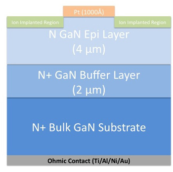
Previous research into developing high power GaN devices ran into obstacles, because large electric fields were created at specific points on the devices' edge when high voltages were applied - effectively destroying the devices. NC State researchers have addressed the problem by implanting a buffer made of the element argon at the edges of GaN devices. The buffer spreads out the electric field, allowing the device to handle much higher voltages.
The researchers tested the new technique on Schottky diodes - common electronic components - and found that the argon implant allowed the GaN diodes to handle almost seven times higher voltages. The diodes that did not have the argon implant broke down when exposed to approximately 250 volts. The diodes with the argon implant could handle up to 1,650 volts before breaking down.
"By improving the breakdown voltage from 250 volts to 1,650 volts, we can reduce the electrical resistance of these devices a hundredfold," says Dr. Jay Baliga, Distinguished University Professor of Electrical and Computer Engineering at NC State and co-author of the paper. "That reduction in resistance means that these devices can handle ten times as much power."
The paper, "Planar, Nearly Ideal Edge Termination Technique for GaN Devices," is forthcoming from IEEE's Electron Device Letters. The research was supported by NC State's Future Renewable Electric Energy Delivery and Management Systems Center, with funding from the National Science Foundation.
NC State's Department of Electrical and Computer Engineering is part of the university's College of Engineering.
Abstract
"Planar, Nearly Ideal Edge Termination Technique for GaN Devices"
Authors: A. Merve Ozbek, B. Jayant Baliga, North Carolina State University
Published: Forthcoming, Electron Device Letters
Abstract: In this paper, a simple edge termination is described which can be used to achieve nearly ideal parallel plane breakdown voltage for GaN devices. This technique involves implanting a neutral species on the edges of devices to form a high resistive amorphous layer. With this termination, formed by using argon implantation, the breakdown voltage of GaN Schottky barrier diodes were increased from 300V for unterminated diodes to 1650V after termination.
####
For more information, please click here
Contacts:
Matt Shipman
News Services
919.515.6386
Dr. Jay Baliga
919.515.6169
Copyright © North Carolina State University
If you have a comment, please Contact us.Issuers of news releases, not 7th Wave, Inc. or Nanotechnology Now, are solely responsible for the accuracy of the content.
Bookmark:


| Related News Press |
News and information
![]() Quantum computer improves AI predictions April 17th, 2026
Quantum computer improves AI predictions April 17th, 2026
![]() Flexible sensor gains sensitivity under pressure April 17th, 2026
Flexible sensor gains sensitivity under pressure April 17th, 2026
![]() A reusable chip for particulate matter sensing April 17th, 2026
A reusable chip for particulate matter sensing April 17th, 2026
![]() Detecting vibrational quantum beating in the predissociation dynamics of SF6 using time-resolved photoelectron spectroscopy April 17th, 2026
Detecting vibrational quantum beating in the predissociation dynamics of SF6 using time-resolved photoelectron spectroscopy April 17th, 2026
Govt.-Legislation/Regulation/Funding/Policy
![]() Quantum computer improves AI predictions April 17th, 2026
Quantum computer improves AI predictions April 17th, 2026
![]() Metasurfaces smooth light to boost magnetic sensing precision January 30th, 2026
Metasurfaces smooth light to boost magnetic sensing precision January 30th, 2026
![]() New imaging approach transforms study of bacterial biofilms August 8th, 2025
New imaging approach transforms study of bacterial biofilms August 8th, 2025
Possible Futures
![]() A fundamentally new therapeutic approach to cystic fibrosis: Nanobody repairs cellular defect April 17th, 2026
A fundamentally new therapeutic approach to cystic fibrosis: Nanobody repairs cellular defect April 17th, 2026
![]() UC Irvine physicists discover method to reverse �quantum scrambling� : The work addresses the problem of information loss in quantum computing system April 17th, 2026
UC Irvine physicists discover method to reverse �quantum scrambling� : The work addresses the problem of information loss in quantum computing system April 17th, 2026
Academic/Education
![]() Rice University launches Rice Synthetic Biology Institute to improve lives January 12th, 2024
Rice University launches Rice Synthetic Biology Institute to improve lives January 12th, 2024
![]() Multi-institution, $4.6 million NSF grant to fund nanotechnology training September 9th, 2022
Multi-institution, $4.6 million NSF grant to fund nanotechnology training September 9th, 2022
Chip Technology
![]() A reusable chip for particulate matter sensing April 17th, 2026
A reusable chip for particulate matter sensing April 17th, 2026
![]() Metasurfaces smooth light to boost magnetic sensing precision January 30th, 2026
Metasurfaces smooth light to boost magnetic sensing precision January 30th, 2026
Nanoelectronics
![]() Lab to industry: InSe wafer-scale breakthrough for future electronics August 8th, 2025
Lab to industry: InSe wafer-scale breakthrough for future electronics August 8th, 2025
![]() Interdisciplinary: Rice team tackles the future of semiconductors Multiferroics could be the key to ultralow-energy computing October 6th, 2023
Interdisciplinary: Rice team tackles the future of semiconductors Multiferroics could be the key to ultralow-energy computing October 6th, 2023
![]() Key element for a scalable quantum computer: Physicists from Forschungszentrum J�lich and RWTH Aachen University demonstrate electron transport on a quantum chip September 23rd, 2022
Key element for a scalable quantum computer: Physicists from Forschungszentrum J�lich and RWTH Aachen University demonstrate electron transport on a quantum chip September 23rd, 2022
![]() Reduced power consumption in semiconductor devices September 23rd, 2022
Reduced power consumption in semiconductor devices September 23rd, 2022
Announcements
![]() A fundamentally new therapeutic approach to cystic fibrosis: Nanobody repairs cellular defect April 17th, 2026
A fundamentally new therapeutic approach to cystic fibrosis: Nanobody repairs cellular defect April 17th, 2026
![]() UC Irvine physicists discover method to reverse �quantum scrambling� : The work addresses the problem of information loss in quantum computing system April 17th, 2026
UC Irvine physicists discover method to reverse �quantum scrambling� : The work addresses the problem of information loss in quantum computing system April 17th, 2026
|
|
||
|
|
||
| The latest news from around the world, FREE | ||
|
|
||
|
|
||
| Premium Products | ||
|
|
||
|
Only the news you want to read!
Learn More |
||
|
|
||
|
Full-service, expert consulting
Learn More |
||
|
|
||