Home > Press > ORNL scientists crack materials mystery in vanadium dioxide
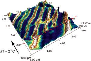 |
| Theoretical research at Oak Ridge National Laboratory can help explain experimental results in vanadium dioxide, such as the formation of thin conductive channels (seen in white) that can appear under strain in a nanoscale vanadium dioxide sample. |
Abstract:
A systematic study of phase changes in vanadium dioxide has solved a mystery that has puzzled scientists for decades, according to researchers at the Department of Energy's Oak Ridge National Laboratory.
ORNL scientists crack materials mystery in vanadium dioxide
Oak Ridge, TN | Posted on November 24th, 2010Scientists have known that vanadium dioxide exhibits several competing phases when it acts as an insulator at lower temperatures. However, the exact nature of the phase behavior has not been understood since research began on vanadium dioxide in the early 1960s.
Alexander Tselev, a research associate from the University of Tennessee-Knoxville working with ORNL's Center for Nanophase Materials Sciences, in collaboration with Igor Luk'yanchuk from the University of Picardy in France used a condensed matter physics theory to explain the observed phase behaviors of vanadium dioxide, a material of significant technological interest for optics and electronics.
"We discovered that the competition between several phases is purely driven by the lattice symmetry," Tselev said. "We figured out that the metallic phase lattice of vanadium oxide can 'fold' in different ways while cooling, so what people observed was different types of its folding."
Vanadium dioxide is best known in the materials world for its speedy and abrupt phase transition that essentially transforms the material from a metal to an insulator. The phase change takes place at about 68 degrees Celsius.
"These features of electrical conductivity make vanadium dioxide an excellent candidate for numerous applications in optical, electronic and optoelectronic devices," Tselev said.
Devices that might take advantage of the unusual properties of VO2 include lasers, motion detectors and pressure detectors, which could benefit from the increased sensitivity provided by the property changes of vanadium dioxide. The material is already used in technologies such as infrared sensors.
Researchers said their theoretical work could help guide future experimental research in vanadium dioxide and ultimately aid the development of new technologies based on VO2.
"In physics, you always want to understand how the material ticks," said Sergei Kalinin, a senior scientist at the CNMS. "The thermodynamic theory will allow you to predict how the material will behave in different external conditions."
The results were published in the American Chemical Society's Nano Letters. The research team also included Ilia Ivanov, John Budai and Jonathan Tischler at ORNL and Evgheni Strelcov and Andrei Kolmakov at Southern Illinois University.
The team's theoretical research expands upon previous experimental ORNL studies with microwave imaging that demonstrated how strain and changes of crystal lattice symmetry can produce thin conductive wires in nanoscale vanadium dioxide samples.
This research was supported in part by the Department of Energy's Office of Science and by the National Science Foundation. Researchers also used instrumentation at the Office of Science-supported Center for Nanophase Materials Sciences and Advanced Photon Source User Facilities at Oak Ridge and Argonne national laboratories, respectively.
####
About Oak Ridge National Laboratory
CNMS is one of the five DOE Nanoscale Science Research Centers, premier national user facilities for interdisciplinary research at the nanoscale supported by the DOE Office of Science. Together the NSRCs comprise a suite of complementary facilities that provide researchers with state-of-the-art capabilities to fabricate, process, characterize and model nanoscale materials, and constitute the largest infrastructure investment of the National Nanotechnology Initiative. The NSRCs are located at DOE's Argonne, Brookhaven, Lawrence Berkeley, Oak Ridge and Sandia and Los Alamos National Laboratories. For more information about the DOE NSRCs, please visit nano.energy.gov. ORNL is managed by UT-Battelle for the Department of Energy's Office of Science.
For more information, please click here
Contacts:
Media Contact: Morgan McCorkle
Communications and External Relations
865.574.7308
Copyright © Oak Ridge National Laboratory
If you have a comment, please Contact us.Issuers of news releases, not 7th Wave, Inc. or Nanotechnology Now, are solely responsible for the accuracy of the content.
Bookmark:


| Related News Press |
News and information
![]() Quantum computer improves AI predictions April 17th, 2026
Quantum computer improves AI predictions April 17th, 2026
![]() Flexible sensor gains sensitivity under pressure April 17th, 2026
Flexible sensor gains sensitivity under pressure April 17th, 2026
![]() A reusable chip for particulate matter sensing April 17th, 2026
A reusable chip for particulate matter sensing April 17th, 2026
![]() Detecting vibrational quantum beating in the predissociation dynamics of SF6 using time-resolved photoelectron spectroscopy April 17th, 2026
Detecting vibrational quantum beating in the predissociation dynamics of SF6 using time-resolved photoelectron spectroscopy April 17th, 2026
Physics
![]() UC Irvine physicists discover method to reverse �quantum scrambling� : The work addresses the problem of information loss in quantum computing system April 17th, 2026
UC Irvine physicists discover method to reverse �quantum scrambling� : The work addresses the problem of information loss in quantum computing system April 17th, 2026
![]() Quantum computers simulate fundamental physics: shedding light on the building blocks of nature June 6th, 2025
Quantum computers simulate fundamental physics: shedding light on the building blocks of nature June 6th, 2025
Govt.-Legislation/Regulation/Funding/Policy
![]() Quantum computer improves AI predictions April 17th, 2026
Quantum computer improves AI predictions April 17th, 2026
![]() Metasurfaces smooth light to boost magnetic sensing precision January 30th, 2026
Metasurfaces smooth light to boost magnetic sensing precision January 30th, 2026
![]() New imaging approach transforms study of bacterial biofilms August 8th, 2025
New imaging approach transforms study of bacterial biofilms August 8th, 2025
Academic/Education
![]() Rice University launches Rice Synthetic Biology Institute to improve lives January 12th, 2024
Rice University launches Rice Synthetic Biology Institute to improve lives January 12th, 2024
![]() Multi-institution, $4.6 million NSF grant to fund nanotechnology training September 9th, 2022
Multi-institution, $4.6 million NSF grant to fund nanotechnology training September 9th, 2022
Nanoelectronics
![]() Lab to industry: InSe wafer-scale breakthrough for future electronics August 8th, 2025
Lab to industry: InSe wafer-scale breakthrough for future electronics August 8th, 2025
![]() Interdisciplinary: Rice team tackles the future of semiconductors Multiferroics could be the key to ultralow-energy computing October 6th, 2023
Interdisciplinary: Rice team tackles the future of semiconductors Multiferroics could be the key to ultralow-energy computing October 6th, 2023
![]() Key element for a scalable quantum computer: Physicists from Forschungszentrum J�lich and RWTH Aachen University demonstrate electron transport on a quantum chip September 23rd, 2022
Key element for a scalable quantum computer: Physicists from Forschungszentrum J�lich and RWTH Aachen University demonstrate electron transport on a quantum chip September 23rd, 2022
![]() Reduced power consumption in semiconductor devices September 23rd, 2022
Reduced power consumption in semiconductor devices September 23rd, 2022
Discoveries
![]() Quantum computer improves AI predictions April 17th, 2026
Quantum computer improves AI predictions April 17th, 2026
![]() Flexible sensor gains sensitivity under pressure April 17th, 2026
Flexible sensor gains sensitivity under pressure April 17th, 2026
![]() A reusable chip for particulate matter sensing April 17th, 2026
A reusable chip for particulate matter sensing April 17th, 2026
![]() Detecting vibrational quantum beating in the predissociation dynamics of SF6 using time-resolved photoelectron spectroscopy April 17th, 2026
Detecting vibrational quantum beating in the predissociation dynamics of SF6 using time-resolved photoelectron spectroscopy April 17th, 2026
Announcements
![]() A fundamentally new therapeutic approach to cystic fibrosis: Nanobody repairs cellular defect April 17th, 2026
A fundamentally new therapeutic approach to cystic fibrosis: Nanobody repairs cellular defect April 17th, 2026
![]() UC Irvine physicists discover method to reverse �quantum scrambling� : The work addresses the problem of information loss in quantum computing system April 17th, 2026
UC Irvine physicists discover method to reverse �quantum scrambling� : The work addresses the problem of information loss in quantum computing system April 17th, 2026
Photonics/Optics/Lasers
![]() Metasurfaces smooth light to boost magnetic sensing precision January 30th, 2026
Metasurfaces smooth light to boost magnetic sensing precision January 30th, 2026
![]() From sensors to smart systems: the rise of AI-driven photonic noses January 30th, 2026
From sensors to smart systems: the rise of AI-driven photonic noses January 30th, 2026
Research partnerships
![]() Lab to industry: InSe wafer-scale breakthrough for future electronics August 8th, 2025
Lab to industry: InSe wafer-scale breakthrough for future electronics August 8th, 2025
![]() HKU physicists uncover hidden order in the quantum world through deconfined quantum critical points April 25th, 2025
HKU physicists uncover hidden order in the quantum world through deconfined quantum critical points April 25th, 2025
|
|
||
|
|
||
| The latest news from around the world, FREE | ||
|
|
||
|
|
||
| Premium Products | ||
|
|
||
|
Only the news you want to read!
Learn More |
||
|
|
||
|
Full-service, expert consulting
Learn More |
||
|
|
||