Home > Press > Researchers Develop Techniques for Using Material Recognized in Nobel Prize
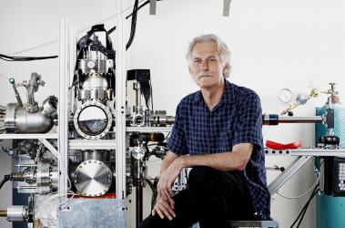 |
| Walt de Heer in laboratory - A team headed by Georgia Tech professor Walt de Heer has pioneered fabrication techniques for producing electronic devices from graphene. (Credit: Mali Azima) |
Abstract:
Georgia Institute of Technology researchers have pioneered the fabrication techniques expected to be used for manufacturing high-performance electronic devices from the material that has been recognized in this year's Nobel Prize in physics.
Researchers Develop Techniques for Using Material Recognized in Nobel Prize
Atlanta, GA | Posted on October 11th, 2010The 2010 physics prize was awarded for producing, isolating, identifying and characterizing graphene, a single atomic layer of carbon whose unique properties make the material attractive for electronic applications. Scientists at the University of Manchester were recognized for their work on graphene sheets peeled from blocks of graphite.
The work of the Georgia Tech group, headed by Professor Walt de Heer in the Georgia Tech School of Physics, was recognized by the Royal Swedish Academy of Sciences in its scientific background document on the physics prize. De Heer's group pioneered epitaxial techniques for growing large-scale graphene sheets by heating wafers of silicon carbide to drive off the silicon, leaving a thin layer of graphene.
The technique, which is now being used by research groups at companies such as IBM, has practical applications in large-scale production of electronic devices. On Oct. 3, the group published a paper in the journal Nature Nanotechnology describing a new technique used to produce an array of 10,000 graphene transistors.
"We believe that our technique, or one very much like it, will ultimately be used to manufacture future generations of graphene-based electronic devices," said de Heer. "Using techniques that are suitable for scaling up for mass production, we can grow graphene in the patterns that we need for electronic devices."
The Georgia Tech group holds a patent, filed in 2003, on fabricating electronic devices from these graphene layers.
Georgia Tech is home to a Materials Research Science and Engineering Center (MRSEC), funded by the National Science Foundation (NSF) and including collaborators from the University of California-Berkeley, University of California-Riverside and University of Michigan. The foundation focus of the center is research and development of epitaxial graphene.
"The unique properties of graphene portend considerable promise for future electronic and optical devices," said Dennis Hess, the center's director. "If graphene is to serve as a viable successor to silicon-based microelectronic devices and circuits, large scale production on a suitable substrate is required. Proof of concept of this approach has already been demonstrated by the fabrication of a 10,000 epitaxial graphene transistor array by Walt de Heer and his collaborators. This achievement is a significant advance toward realizing carbon-based electronics for the 21st century."
The Georgia Tech team also collaborates with researchers at the National Institute of Standards and Technology (NIST) on characterizing the unique properties of graphene. That work has led to several recent important papers, in journals such as Science and Nature Physics. The latter described for the first time how the orbits of electrons are distributed spatially by magnetic fields applied to layers of epitaxial graphene.
On Oct. 3 in the advance online publication of the journal Nature Nanotechnology, de Heer and collaborators described the development of a new "templated growth" technique for fabricating nanometer-scale graphene devices. The method addresses what had been a significant obstacle to the use of this promising material in future generations of high-performance electronic devices.
The technique involves etching patterns into the silicon carbide surfaces on which epitaxial graphene is grown. The patterns serve as templates directing the growth of graphene structures, allowing the formation of nanoribbons of specific widths without the use of e-beams or other destructive cutting techniques. Templated nanoribbon growth addresses the edge roughness that causes electron scattering.
####
For more information, please click here
Contacts:
Media Relations Contacts:
John Toon
404-894-6986
Abby Vogel Robinson
404-385-3364
Copyright © Georgia Institute of Technology
If you have a comment, please Contact us.Issuers of news releases, not 7th Wave, Inc. or Nanotechnology Now, are solely responsible for the accuracy of the content.
Bookmark:


| Related News Press |
News and information
![]() Quantum computer improves AI predictions April 17th, 2026
Quantum computer improves AI predictions April 17th, 2026
![]() Flexible sensor gains sensitivity under pressure April 17th, 2026
Flexible sensor gains sensitivity under pressure April 17th, 2026
![]() A reusable chip for particulate matter sensing April 17th, 2026
A reusable chip for particulate matter sensing April 17th, 2026
![]() Detecting vibrational quantum beating in the predissociation dynamics of SF6 using time-resolved photoelectron spectroscopy April 17th, 2026
Detecting vibrational quantum beating in the predissociation dynamics of SF6 using time-resolved photoelectron spectroscopy April 17th, 2026
Possible Futures
![]() A fundamentally new therapeutic approach to cystic fibrosis: Nanobody repairs cellular defect April 17th, 2026
A fundamentally new therapeutic approach to cystic fibrosis: Nanobody repairs cellular defect April 17th, 2026
![]() UC Irvine physicists discover method to reverse �quantum scrambling� : The work addresses the problem of information loss in quantum computing system April 17th, 2026
UC Irvine physicists discover method to reverse �quantum scrambling� : The work addresses the problem of information loss in quantum computing system April 17th, 2026
Academic/Education
![]() Rice University launches Rice Synthetic Biology Institute to improve lives January 12th, 2024
Rice University launches Rice Synthetic Biology Institute to improve lives January 12th, 2024
![]() Multi-institution, $4.6 million NSF grant to fund nanotechnology training September 9th, 2022
Multi-institution, $4.6 million NSF grant to fund nanotechnology training September 9th, 2022
Chip Technology
![]() A reusable chip for particulate matter sensing April 17th, 2026
A reusable chip for particulate matter sensing April 17th, 2026
![]() Metasurfaces smooth light to boost magnetic sensing precision January 30th, 2026
Metasurfaces smooth light to boost magnetic sensing precision January 30th, 2026
Nanotubes/Buckyballs/Fullerenes/Nanorods/Nanostrings/Nanosheets
![]() Tiny nanosheets, big leap: A new sensor detects ethanol at ultra-low levels January 30th, 2026
Tiny nanosheets, big leap: A new sensor detects ethanol at ultra-low levels January 30th, 2026
![]() Enhancing power factor of p- and n-type single-walled carbon nanotubes April 25th, 2025
Enhancing power factor of p- and n-type single-walled carbon nanotubes April 25th, 2025
![]() Chainmail-like material could be the future of armor: First 2D mechanically interlocked polymer exhibits exceptional flexibility and strength January 17th, 2025
Chainmail-like material could be the future of armor: First 2D mechanically interlocked polymer exhibits exceptional flexibility and strength January 17th, 2025
![]() Innovative biomimetic superhydrophobic coating combines repair and buffering properties for superior anti-erosion December 13th, 2024
Innovative biomimetic superhydrophobic coating combines repair and buffering properties for superior anti-erosion December 13th, 2024
Nanoelectronics
![]() Lab to industry: InSe wafer-scale breakthrough for future electronics August 8th, 2025
Lab to industry: InSe wafer-scale breakthrough for future electronics August 8th, 2025
![]() Interdisciplinary: Rice team tackles the future of semiconductors Multiferroics could be the key to ultralow-energy computing October 6th, 2023
Interdisciplinary: Rice team tackles the future of semiconductors Multiferroics could be the key to ultralow-energy computing October 6th, 2023
![]() Key element for a scalable quantum computer: Physicists from Forschungszentrum J�lich and RWTH Aachen University demonstrate electron transport on a quantum chip September 23rd, 2022
Key element for a scalable quantum computer: Physicists from Forschungszentrum J�lich and RWTH Aachen University demonstrate electron transport on a quantum chip September 23rd, 2022
![]() Reduced power consumption in semiconductor devices September 23rd, 2022
Reduced power consumption in semiconductor devices September 23rd, 2022
Announcements
![]() A fundamentally new therapeutic approach to cystic fibrosis: Nanobody repairs cellular defect April 17th, 2026
A fundamentally new therapeutic approach to cystic fibrosis: Nanobody repairs cellular defect April 17th, 2026
![]() UC Irvine physicists discover method to reverse �quantum scrambling� : The work addresses the problem of information loss in quantum computing system April 17th, 2026
UC Irvine physicists discover method to reverse �quantum scrambling� : The work addresses the problem of information loss in quantum computing system April 17th, 2026
Patents/IP/Tech Transfer/Licensing
![]() Getting drugs across the blood-brain barrier using nanoparticles March 3rd, 2023
Getting drugs across the blood-brain barrier using nanoparticles March 3rd, 2023
![]() Metasurfaces control polarized light at will: New research unlocks the hidden potential of metasurfaces August 13th, 2021
Metasurfaces control polarized light at will: New research unlocks the hidden potential of metasurfaces August 13th, 2021
![]() Arrowhead Pharmaceuticals Announces Closing of Agreement with Takeda November 27th, 2020
Arrowhead Pharmaceuticals Announces Closing of Agreement with Takeda November 27th, 2020
Grants/Sponsored Research/Awards/Scholarships/Gifts/Contests/Honors/Records
![]() Quantum computer improves AI predictions April 17th, 2026
Quantum computer improves AI predictions April 17th, 2026
![]() Detecting vibrational quantum beating in the predissociation dynamics of SF6 using time-resolved photoelectron spectroscopy April 17th, 2026
Detecting vibrational quantum beating in the predissociation dynamics of SF6 using time-resolved photoelectron spectroscopy April 17th, 2026
![]() Metasurfaces smooth light to boost magnetic sensing precision January 30th, 2026
Metasurfaces smooth light to boost magnetic sensing precision January 30th, 2026
Research partnerships
![]() Lab to industry: InSe wafer-scale breakthrough for future electronics August 8th, 2025
Lab to industry: InSe wafer-scale breakthrough for future electronics August 8th, 2025
![]() HKU physicists uncover hidden order in the quantum world through deconfined quantum critical points April 25th, 2025
HKU physicists uncover hidden order in the quantum world through deconfined quantum critical points April 25th, 2025
|
|
||
|
|
||
| The latest news from around the world, FREE | ||
|
|
||
|
|
||
| Premium Products | ||
|
|
||
|
Only the news you want to read!
Learn More |
||
|
|
||
|
Full-service, expert consulting
Learn More |
||
|
|
||