Home > Press > Growing Nanowires Horizontally Yields New Benefit:: 'Nano-LEDs'
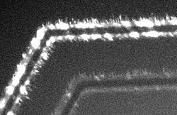 |
| Transmission electron microscope image of “nano LEDs” emitting light.
Credit: NIST |
Abstract:
While refining their novel method for making nanoscale wires, chemists at the National Institute of Standards and Technology (NIST) discovered an unexpected bonus—a new way to create nanowires that produce light similar to that from light-emitting diodes (LEDs). These "nano-LEDs" may one day have their light-emission abilities put to work serving miniature devices such as nanogenerators or lab-on-a-chip systems.
Growing Nanowires Horizontally Yields New Benefit:: 'Nano-LEDs'
Gaithersburg, MD | Posted on September 29th, 2010Nanowires typically are "grown" by the controlled deposition of molecules—zinc oxide, for example—from a gas onto a base material, a process called chemical vapor deposition (CVD). Most CVD techniques form nanowires that rise vertically from the surface like brush bristles. Because the wire only contacts the substrate at one end, it tends not to share characteristics with the substrate material—a less-than-preferred trait because the exact composition of the nanowire will then be hard to define. Vertical growth also produces a dense forest of nanowires, making it difficult to find and re-position individual wires of superior quality. To remedy these shortcomings, NIST chemists Babak Nikoobakht and Andrew Herzing developed a "surface-directed" method for growing nanowires horizontally across the substrate (see "NIST Demos Industrial-Grade Nanowire Device Fabrication" NIST Tech Beat, Oct. 25, 2007, at www.nist.gov/public_affairs/techbeat/tb2007_1025.htm#nanowire).
Like many vertical growth CVD methods, the NIST fabrication technique uses gold as a catalyst for crystal formation. The difference is that the gold deposited in the NIST method is heated to 900 degrees Celsius (1,652 degrees Fahrenheit), converting it to a nanoparticle that serves as growth site and medium for the crystallization of zinc oxide molecules. As the zinc oxide nanocrystal grows, it pushes the gold nanoparticle along the surface of the substrate (in this experiment, gallium nitride) to form a nanowire that grows horizontally across the substrate and so exhibits properties strongly influenced by its base material.
In recent work published in ACS Nano,* Nikoobakht and Herzing increased the thickness of the gold catalyst nanoparticle from less than 8 nanometers to approximately 20 nanometers. The change resulted in nanowires that grew a secondary structure, a shark-like "dorsal fin" (referred to as a "nanowall") where the zinc oxide portion is electron-rich and the gallium nitride portion is electron-poor. The interface between these two materials—known as a p-n heterojunction—allows electrons to flow across it when the nanowire-nanowall combination was charged with electricity. In turn, the movement of electrons produced light and led the researchers to dub it a "nano LED."
Unlike previous techniques for producing heterojunctions, the NIST "surface-directed" fabrication method makes it easy to locate individual heterojunctions on the surface. This feature is especially useful when a large number of heterojunctions must be grouped in an array so that they can be electrically charged as a light-emitting unit.
Transmission electron microscope (TEM) examination of the zinc oxide-gallium nitride nanowires and nanowalls revealed few structural defects in the nanowires and very distinct p-n heterojunctions in the nanowalls, both affirmations of the effectiveness of the NIST "surface directed" fabrication method.
Nikoobakht and Herzing hope to improve the nano LEDs in future experiments using better geometry and material designs, and then apply them in the development of light sources and detectors useful in photonic devices or lab-on-a-chip platforms.
* B. Nikkoobakht and A. Herzing. Formation of planar arrays of one-dimensional p-n heterojunctions using surface-directed growth of nanowires and nanowalls. ACS Nano. Published online Sept. 15, 2010.
####
About NIST
The National Institute of Standards and Technology (NIST) is an agency of the U.S. Commerce Department.
For more information, please click here
Contacts:
Michael E. Newman
301-975-3025
Copyright © NIST
If you have a comment, please Contact us.Issuers of news releases, not 7th Wave, Inc. or Nanotechnology Now, are solely responsible for the accuracy of the content.
Bookmark:


| Related News Press |
News and information
![]() Quantum computer improves AI predictions April 17th, 2026
Quantum computer improves AI predictions April 17th, 2026
![]() Flexible sensor gains sensitivity under pressure April 17th, 2026
Flexible sensor gains sensitivity under pressure April 17th, 2026
![]() A reusable chip for particulate matter sensing April 17th, 2026
A reusable chip for particulate matter sensing April 17th, 2026
![]() Detecting vibrational quantum beating in the predissociation dynamics of SF6 using time-resolved photoelectron spectroscopy April 17th, 2026
Detecting vibrational quantum beating in the predissociation dynamics of SF6 using time-resolved photoelectron spectroscopy April 17th, 2026
Display technology/LEDs/SS Lighting/OLEDs
![]() Spinel-type sulfide semiconductors to operate the next-generation LEDs and solar cells For solar-cell absorbers and green-LED source October 3rd, 2025
Spinel-type sulfide semiconductors to operate the next-generation LEDs and solar cells For solar-cell absorbers and green-LED source October 3rd, 2025
![]() Efficient and stable hybrid perovskite-organic light-emitting diodes with external quantum efficiency exceeding 40 per cent July 5th, 2024
Efficient and stable hybrid perovskite-organic light-emitting diodes with external quantum efficiency exceeding 40 per cent July 5th, 2024
Govt.-Legislation/Regulation/Funding/Policy
![]() Quantum computer improves AI predictions April 17th, 2026
Quantum computer improves AI predictions April 17th, 2026
![]() Metasurfaces smooth light to boost magnetic sensing precision January 30th, 2026
Metasurfaces smooth light to boost magnetic sensing precision January 30th, 2026
![]() New imaging approach transforms study of bacterial biofilms August 8th, 2025
New imaging approach transforms study of bacterial biofilms August 8th, 2025
Discoveries
![]() Quantum computer improves AI predictions April 17th, 2026
Quantum computer improves AI predictions April 17th, 2026
![]() Flexible sensor gains sensitivity under pressure April 17th, 2026
Flexible sensor gains sensitivity under pressure April 17th, 2026
![]() A reusable chip for particulate matter sensing April 17th, 2026
A reusable chip for particulate matter sensing April 17th, 2026
![]() Detecting vibrational quantum beating in the predissociation dynamics of SF6 using time-resolved photoelectron spectroscopy April 17th, 2026
Detecting vibrational quantum beating in the predissociation dynamics of SF6 using time-resolved photoelectron spectroscopy April 17th, 2026
Announcements
![]() A fundamentally new therapeutic approach to cystic fibrosis: Nanobody repairs cellular defect April 17th, 2026
A fundamentally new therapeutic approach to cystic fibrosis: Nanobody repairs cellular defect April 17th, 2026
![]() UC Irvine physicists discover method to reverse ‘quantum scrambling’ : The work addresses the problem of information loss in quantum computing system April 17th, 2026
UC Irvine physicists discover method to reverse ‘quantum scrambling’ : The work addresses the problem of information loss in quantum computing system April 17th, 2026
Energy
![]() Sensors innovations for smart lithium-based batteries: advancements, opportunities, and potential challenges August 8th, 2025
Sensors innovations for smart lithium-based batteries: advancements, opportunities, and potential challenges August 8th, 2025
![]() Simple algorithm paired with standard imaging tool could predict failure in lithium metal batteries August 8th, 2025
Simple algorithm paired with standard imaging tool could predict failure in lithium metal batteries August 8th, 2025
Battery Technology/Capacitors/Generators/Piezoelectrics/Thermoelectrics/Energy storage
![]() Decoding hydrogen‑bond network of electrolyte for cryogenic durable aqueous zinc‑ion batteries January 30th, 2026
Decoding hydrogen‑bond network of electrolyte for cryogenic durable aqueous zinc‑ion batteries January 30th, 2026
![]() COF scaffold membrane with gate‑lane nanostructure for efficient Li+/Mg2+ separation January 30th, 2026
COF scaffold membrane with gate‑lane nanostructure for efficient Li+/Mg2+ separation January 30th, 2026
![]() MXene nanomaterials enter a new dimension Multilayer nanomaterial: MXene flakes created at Drexel University show new promise as 1D scrolls January 30th, 2026
MXene nanomaterials enter a new dimension Multilayer nanomaterial: MXene flakes created at Drexel University show new promise as 1D scrolls January 30th, 2026
|
|
||
|
|
||
| The latest news from around the world, FREE | ||
|
|
||
|
|
||
| Premium Products | ||
|
|
||
|
Only the news you want to read!
Learn More |
||
|
|
||
|
Full-service, expert consulting
Learn More |
||
|
|
||