Home > Press > Unprecedented look at oxide interfaces reveals unexpected structures on atomic scale
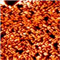 |
| A new scanning tunneling microscopy and low energy electron diffraction technique developed at Oak Ridge National Laboratory captured this 50 nm x 50 nm image of an oxide surface. Each bright dot is a single atom of material. |
Abstract:
Thin layers of oxide materials and their interfaces have been observed in atomic resolution during growth for the first time by researchers at the Center for Nanophase Materials Sciences at the Department of Energy's Oak Ridge National Laboratory, providing new insight into the complicated link between their structure and properties.
Unprecedented look at oxide interfaces reveals unexpected structures on atomic scale
Oak Ridge, TN | Posted on August 9th, 2010"Imagine you suddenly had the ability to see in color, or in 3-D," said the CNMS's Sergei Kalinin. "That is how close we have been able to look at these very small interfaces."
The paper was published online in ACS Nano with ORNL's Junsoo Shin as lead author.
A component of magnetoelectronics and spintronics, oxide interfaces have the potential to replace silicon-based microelectronic devices and improve the power and memory retention of other electronic technologies.
However, oxide interfaces are difficult to analyze at the atomic scale because once the oxides are removed from their growth chamber they become contaminated. To circumvent this problem, ORNL researchers led by Art Baddorf built a unique system that allows scanning tunneling microscopy and low energy electron diffraction to capture images of the top layer of the oxide while in situ, or still in the vacuum chamber where the materials were grown by powerful laser pulses.
Many studies of similar oxide interfaces utilize a look from the side, typically achieved by aberration corrected scanning transmission electron microscopy (STEM). The ORNL team has used these cross-sectional images to map the oxide organization.
However, like a sandwich, oxide interfaces may be more than what they appear from the side. In order to observe the interactive layer of the top and bottom oxide, the group has used scanning tunneling microscopy to get an atomically resolved view of the surface of the oxide, and observed its evolution during the growth of a second oxide film on top.
"Instead of seeing a perfectly flat, square lattice that scientists thought these interfaces were before, we found a different and very complicated atomic ordering," said Baddorf. "We really need to reassess what we know about these materials."
Oxides can be used in different combinations to produce unique results. For instance, isolated, two oxides may be insulators but together the interface may become conductive. By viewing the atomic structure of one oxide, scientists can more effectively couple oxides to perform optimally in advanced technological applications such as transistors.
Kalinin says the correct application of these interface-based materials may open new pathways for development of computer processors and energy storage and conversion devices, as well as understanding basic physics controlling these materials.
"In the last 10 years, there has been only limited progress in developing beyond-silicon information technologies," Kalinin said. "Silicon has limitations that have been reached, and this has motivated people to explore other options."
Atomic resolution of interface structures during oxide growth will better enable scientists to identify defects of certain popular oxide combinations and could help narrow selections of oxides to spur new or more efficient commercial applications.
This research is supported by the U.S. Department of Energy, Office of Science.
####
About Oak Ridge National Laboratory
The Center for Nanophase Materials Sciences at ORNL is one of the five DOE Nanoscale Science Research Centers supported by the DOE Office of Science, premier national user facilities for interdisciplinary research at the nanoscale. Together the NSRCs comprise a suite of complementary facilities that provide researchers with state-of-the-art capabilities to fabricate, process, characterize and model nanoscale materials, and constitute the largest infrastructure investment of the National Nanotechnology Initiative. The NSRCs are located at DOE's Argonne, Brookhaven, Lawrence Berkeley, Oak Ridge and Sandia and Los Alamos national laboratories. For more information about the DOE NSRCs, please visit http://nano.energy.gov.
ORNL is managed by UT-Battelle for the Department of Energy's Office of Science.
For more information, please click here
Contacts:
Media Contact: Katie Freeman
Communications and External Relations
865.574.6110
Copyright © Oak Ridge National Laboratory
If you have a comment, please Contact us.Issuers of news releases, not 7th Wave, Inc. or Nanotechnology Now, are solely responsible for the accuracy of the content.
Bookmark:


| Related News Press |
News and information
![]() Quantum computer improves AI predictions April 17th, 2026
Quantum computer improves AI predictions April 17th, 2026
![]() Flexible sensor gains sensitivity under pressure April 17th, 2026
Flexible sensor gains sensitivity under pressure April 17th, 2026
![]() A reusable chip for particulate matter sensing April 17th, 2026
A reusable chip for particulate matter sensing April 17th, 2026
![]() Detecting vibrational quantum beating in the predissociation dynamics of SF6 using time-resolved photoelectron spectroscopy April 17th, 2026
Detecting vibrational quantum beating in the predissociation dynamics of SF6 using time-resolved photoelectron spectroscopy April 17th, 2026
Govt.-Legislation/Regulation/Funding/Policy
![]() Quantum computer improves AI predictions April 17th, 2026
Quantum computer improves AI predictions April 17th, 2026
![]() Metasurfaces smooth light to boost magnetic sensing precision January 30th, 2026
Metasurfaces smooth light to boost magnetic sensing precision January 30th, 2026
![]() New imaging approach transforms study of bacterial biofilms August 8th, 2025
New imaging approach transforms study of bacterial biofilms August 8th, 2025
Possible Futures
![]() A fundamentally new therapeutic approach to cystic fibrosis: Nanobody repairs cellular defect April 17th, 2026
A fundamentally new therapeutic approach to cystic fibrosis: Nanobody repairs cellular defect April 17th, 2026
![]() UC Irvine physicists discover method to reverse �quantum scrambling� : The work addresses the problem of information loss in quantum computing system April 17th, 2026
UC Irvine physicists discover method to reverse �quantum scrambling� : The work addresses the problem of information loss in quantum computing system April 17th, 2026
Academic/Education
![]() Rice University launches Rice Synthetic Biology Institute to improve lives January 12th, 2024
Rice University launches Rice Synthetic Biology Institute to improve lives January 12th, 2024
![]() Multi-institution, $4.6 million NSF grant to fund nanotechnology training September 9th, 2022
Multi-institution, $4.6 million NSF grant to fund nanotechnology training September 9th, 2022
Memory Technology
![]() Researchers tackle the memory bottleneck stalling quantum computing October 3rd, 2025
Researchers tackle the memory bottleneck stalling quantum computing October 3rd, 2025
![]() First real-time observation of two-dimensional melting process: Researchers at Mainz University unveil new insights into magnetic vortex structures August 8th, 2025
First real-time observation of two-dimensional melting process: Researchers at Mainz University unveil new insights into magnetic vortex structures August 8th, 2025
![]() Utilizing palladium for addressing contact issues of buried oxide thin film transistors April 5th, 2024
Utilizing palladium for addressing contact issues of buried oxide thin film transistors April 5th, 2024
Announcements
![]() A fundamentally new therapeutic approach to cystic fibrosis: Nanobody repairs cellular defect April 17th, 2026
A fundamentally new therapeutic approach to cystic fibrosis: Nanobody repairs cellular defect April 17th, 2026
![]() UC Irvine physicists discover method to reverse �quantum scrambling� : The work addresses the problem of information loss in quantum computing system April 17th, 2026
UC Irvine physicists discover method to reverse �quantum scrambling� : The work addresses the problem of information loss in quantum computing system April 17th, 2026
|
|
||
|
|
||
| The latest news from around the world, FREE | ||
|
|
||
|
|
||
| Premium Products | ||
|
|
||
|
Only the news you want to read!
Learn More |
||
|
|
||
|
Full-service, expert consulting
Learn More |
||
|
|
||