Home > Press > Imec reports breakthrough for next-generation vertical Flash memories
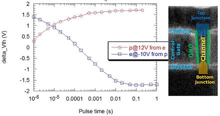 |
| Figure Vertical Flash transistor: Program/erase characteristics on a vertical charge trap Flash cell with poly-Si substrate and corresponding cross-section |
Abstract:
Imec realized a vertical Flash transistor with Si plug diameters down to 20nm. The associated vertical Flash platform paves the way to scale Flash memory to the next nodes. The vertical device concept features enhanced performance at lower voltages as well as reduced cost.
Imec reports breakthrough for next-generation vertical Flash memories
Belgium | Posted on June 22nd, 2010Floating gate Flash memory has been scaling at a tremendous pace in recent years to arrive at a startling density of 32 gigabit (4 gigabyte) on a single die today, using 30nm technology and below. Drastic device concept changes are however required for future generations to cope with the scaling limits of today's floating gate technology. For example the electrostatic cell-to-cell interference and the low storage electron count are becoming major obstacles for further downscaling in the 20 and 10nm range.
Stacking cells in a vertical way on a chip, hence increasing the density per unit area by e.g. 8-16 for the same technology node, is a very promising approach to further push the cost down. Besides cost reduction, vertical stacking also improves the gate control and the field enhancement in the tunnel oxide because of the curvature of the gate-all-around structure. This leads to enhanced window and drive current even in the case of a poly-Si SONOS (silicon oxide nitride oxide silicon) device.
Imec designed a new process flow and all necessary test structures to optimize the vertical transistor flow. The process flow provides a gate layer and inter-gate isolation layers, which are etched all the way down to the Si (to form the so-called �plug'). Next, the ONO (oxide nitride oxide) memory gate stack is deposited on the sidewalls and the plug is filled with poly-Si which serves as the transistor substrate.
Plug opening, bottom junction as well as top junction profile and plug fill were found to be critical steps. Cylindrical cell structures have been obtained with Si diameters down to 20nm. A new process has been developed to allow the removal of the ONO stack at the bottom of the plug for source junction formation without damaging the tunnel oxide on the sidewalls.
Imec's vertical Flash transistor platform will be used to investigate the scalability of this concept for the generations corresponding to the planar 1x nodes. Further experiments will include the reduction of the cell diameter, the selection of the best ONO stack taking topography into account as well as alternative channel processing schemes.
These results were obtained in collaboration with imec's key partners in sub-22nm core CMOS research.
####
About imec
Imec is Europe�s largest independent research center in nanoelectronics and nano-technology. Its staff of more than 1,750 people includes over 550 industrial residents and guest researchers. Imec�s research is applied in better healthcare, smart electronics, sustainable energy, and safer transport.
For more information, please click here
Contacts:
Kapeldreef 75
B-3001 Leuven
Belgium
Phone: +32 16 28 12 11
Fax: +32 16 22 94 00
Copyright © imec
If you have a comment, please Contact us.Issuers of news releases, not 7th Wave, Inc. or Nanotechnology Now, are solely responsible for the accuracy of the content.
Bookmark:


| Related News Press |
News and information
![]() Quantum computer improves AI predictions April 17th, 2026
Quantum computer improves AI predictions April 17th, 2026
![]() Flexible sensor gains sensitivity under pressure April 17th, 2026
Flexible sensor gains sensitivity under pressure April 17th, 2026
![]() A reusable chip for particulate matter sensing April 17th, 2026
A reusable chip for particulate matter sensing April 17th, 2026
![]() Detecting vibrational quantum beating in the predissociation dynamics of SF6 using time-resolved photoelectron spectroscopy April 17th, 2026
Detecting vibrational quantum beating in the predissociation dynamics of SF6 using time-resolved photoelectron spectroscopy April 17th, 2026
Display technology/LEDs/SS Lighting/OLEDs
![]() Spinel-type sulfide semiconductors to operate the next-generation LEDs and solar cells For solar-cell absorbers and green-LED source October 3rd, 2025
Spinel-type sulfide semiconductors to operate the next-generation LEDs and solar cells For solar-cell absorbers and green-LED source October 3rd, 2025
![]() Efficient and stable hybrid perovskite-organic light-emitting diodes with external quantum efficiency exceeding 40 per cent July 5th, 2024
Efficient and stable hybrid perovskite-organic light-emitting diodes with external quantum efficiency exceeding 40 per cent July 5th, 2024
Chip Technology
![]() A reusable chip for particulate matter sensing April 17th, 2026
A reusable chip for particulate matter sensing April 17th, 2026
![]() Metasurfaces smooth light to boost magnetic sensing precision January 30th, 2026
Metasurfaces smooth light to boost magnetic sensing precision January 30th, 2026
Memory Technology
![]() Researchers tackle the memory bottleneck stalling quantum computing October 3rd, 2025
Researchers tackle the memory bottleneck stalling quantum computing October 3rd, 2025
![]() First real-time observation of two-dimensional melting process: Researchers at Mainz University unveil new insights into magnetic vortex structures August 8th, 2025
First real-time observation of two-dimensional melting process: Researchers at Mainz University unveil new insights into magnetic vortex structures August 8th, 2025
![]() Utilizing palladium for addressing contact issues of buried oxide thin film transistors April 5th, 2024
Utilizing palladium for addressing contact issues of buried oxide thin film transistors April 5th, 2024
Nanoelectronics
![]() Lab to industry: InSe wafer-scale breakthrough for future electronics August 8th, 2025
Lab to industry: InSe wafer-scale breakthrough for future electronics August 8th, 2025
![]() Interdisciplinary: Rice team tackles the future of semiconductors Multiferroics could be the key to ultralow-energy computing October 6th, 2023
Interdisciplinary: Rice team tackles the future of semiconductors Multiferroics could be the key to ultralow-energy computing October 6th, 2023
![]() Key element for a scalable quantum computer: Physicists from Forschungszentrum J�lich and RWTH Aachen University demonstrate electron transport on a quantum chip September 23rd, 2022
Key element for a scalable quantum computer: Physicists from Forschungszentrum J�lich and RWTH Aachen University demonstrate electron transport on a quantum chip September 23rd, 2022
![]() Reduced power consumption in semiconductor devices September 23rd, 2022
Reduced power consumption in semiconductor devices September 23rd, 2022
Announcements
![]() A fundamentally new therapeutic approach to cystic fibrosis: Nanobody repairs cellular defect April 17th, 2026
A fundamentally new therapeutic approach to cystic fibrosis: Nanobody repairs cellular defect April 17th, 2026
![]() UC Irvine physicists discover method to reverse �quantum scrambling� : The work addresses the problem of information loss in quantum computing system April 17th, 2026
UC Irvine physicists discover method to reverse �quantum scrambling� : The work addresses the problem of information loss in quantum computing system April 17th, 2026
|
|
||
|
|
||
| The latest news from around the world, FREE | ||
|
|
||
|
|
||
| Premium Products | ||
|
|
||
|
Only the news you want to read!
Learn More |
||
|
|
||
|
Full-service, expert consulting
Learn More |
||
|
|
||