Home > Press > The World’s First Diamond Nanoprobe Tips Demonstrate Success in Nanomanufacturing
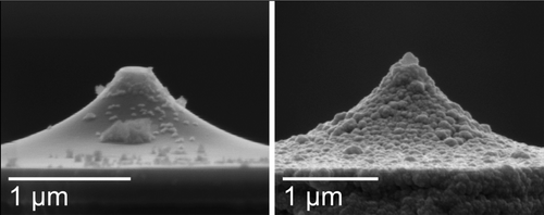 |
| The resistively heated probe can reach temperatures above 600 °C. The batch fabrication process produces UNCD tips with radii as small as 15 nm, with average radius 50 nm across the entire wafer. Wear tests were performed on substrates of quartz, silicon carbide, silicon, or UNCD. Tips were scanned for more than 1 m at a scan speed of 25 μm s−1 at temperatures ranging from 25 to 400 °C under loads up to 200 nN. Credit: ACS |
Abstract:
Advanced Diamond Technologies (ADT), the Univ. of Illinois at Urbana-Champaign, the Naval Research Laboratory, and the Univ. of Pennsylvania have published groundbreaking work in the May 2010 issue of the journal ACS Nano demonstrating that nanometer-scale diamond tips exhibit stability and anti-fouling capabilities under extremely harsh conditions.
The World’s First Diamond Nanoprobe Tips Demonstrate Success in Nanomanufacturing
Romeoville, IL | Posted on June 18th, 2010"Wear-resistant Diamond Nanoprobe Tips with Integrated Silicon Heater for Tip-Based Nanomanufacturing," demonstrates the ability of UNCD tips integrated with doped silicon atomic force microscope (AFM) cantilevers for use in nanomanufacturing. The initial UNCD tip radius can be as small as 15 nm, and retains its shape when scanned for more than a meter at high temperatures and under high loading forces. Silicon tips, frequently used in prototype nanomanufacturing demonstrations, are quickly destroyed under similar conditions. Additionally, silicon tips easily foul, or pick up undesirable material from the scanned surface, while the low stiction properties of diamond avoid fouling.
"The UNCD probe tip, integrated onto a silicon heater-thermometer, has extraordinary longevity and demonstrates success under the harsh conditions required for tip-based nanofabrication," said team leader Dr. William P. King, associate professor and Willett Faculty Scholar at the Univ. of Illinois. "There are countless applications where we would like to have a nanoprobe scan over a hard surface at high temperature and high loading force."
Tip-based nanofabrication is the ability to use a nanometer-scale tip to imprint or write patterns onto a material; which is comparable to using a pencil to write on paper. In the nanoworld, writing tiny patterns is extremely difficult. Tip-based nanomanufacturing is currently used to fabricate or repair nanoelectronics or lithographic masks; a demanding job requiring the tip to scan long distances over hard substances.
"Diamond has long been considered the ideal tip material. This paper demonstrates how UNCD technology meets the challenge of demanding specifications of imaging and nanomaufacturing placed on the tip radius of dimensional stability; thus paving the way for probe-based technologies for a number of applications," said Dr. John Carlisle, chief technology officer, ADT.
These wear resistant diamond nanoprobe tips integrated with silicon heaters are perfectly suited for nanomaterials characterization, nanoscale transport measurements, and applications such as dip-pen nanolithography, probe-based non-volatile memories, and patterning nanowires on surfaces.
Next, the researchers will be building and using arrays of these probe tips. "The longevity of these probes allow them to be implemented in massively parallel arrays that could scan over long distances and at high speed," said Dr. King. "We can now think about using nanoprobe tip arrays to address many square centimeters of surface area. Eventually we'll go to nanoprobe scans on a meter scale."
ADT and its university partners gratefully acknowledge DARPA's Tip-Based Nanofabrication Program for sponsoring this work.
Study abstract
pubs.acs.org/doi/abs/10.1021/nn100203d?prevSearch=%255Bauthor%253A%2BKing%255D&searchHistoryKey
####
About Advanced Diamond Technologies
ADT is the world leader in the development of diamond for industrial, electronics, energy, and medical applications. ADT is a World Economic Forum 2007 Technology Pioneer, a recipient of a 2008 EuroAsia IC Award in the Materials Enabling category from EuroAsia Semiconductor magazine, and a 2008 R&D 100 Award winner for UNCD Seals (mechanical seals for pumps), and a 2009 R&D 100 Award winner for NaDiaProbes® (the world’s first all‐diamond AFM probes).
For more information, please click here
Contacts:
PR Contact
Jill Jackson
Calyx Consulting
312.231.9870
Copyright © Advanced Diamond Technologies
If you have a comment, please Contact us.Issuers of news releases, not 7th Wave, Inc. or Nanotechnology Now, are solely responsible for the accuracy of the content.
Bookmark:


| Related News Press |
Govt.-Legislation/Regulation/Funding/Policy
![]() Quantum computer improves AI predictions April 17th, 2026
Quantum computer improves AI predictions April 17th, 2026
![]() Metasurfaces smooth light to boost magnetic sensing precision January 30th, 2026
Metasurfaces smooth light to boost magnetic sensing precision January 30th, 2026
![]() New imaging approach transforms study of bacterial biofilms August 8th, 2025
New imaging approach transforms study of bacterial biofilms August 8th, 2025
Possible Futures
![]() A fundamentally new therapeutic approach to cystic fibrosis: Nanobody repairs cellular defect April 17th, 2026
A fundamentally new therapeutic approach to cystic fibrosis: Nanobody repairs cellular defect April 17th, 2026
![]() UC Irvine physicists discover method to reverse ‘quantum scrambling’ : The work addresses the problem of information loss in quantum computing system April 17th, 2026
UC Irvine physicists discover method to reverse ‘quantum scrambling’ : The work addresses the problem of information loss in quantum computing system April 17th, 2026
Academic/Education
![]() Rice University launches Rice Synthetic Biology Institute to improve lives January 12th, 2024
Rice University launches Rice Synthetic Biology Institute to improve lives January 12th, 2024
![]() Multi-institution, $4.6 million NSF grant to fund nanotechnology training September 9th, 2022
Multi-institution, $4.6 million NSF grant to fund nanotechnology training September 9th, 2022
Nanoelectronics
![]() Lab to industry: InSe wafer-scale breakthrough for future electronics August 8th, 2025
Lab to industry: InSe wafer-scale breakthrough for future electronics August 8th, 2025
![]() Interdisciplinary: Rice team tackles the future of semiconductors Multiferroics could be the key to ultralow-energy computing October 6th, 2023
Interdisciplinary: Rice team tackles the future of semiconductors Multiferroics could be the key to ultralow-energy computing October 6th, 2023
![]() Key element for a scalable quantum computer: Physicists from Forschungszentrum Jülich and RWTH Aachen University demonstrate electron transport on a quantum chip September 23rd, 2022
Key element for a scalable quantum computer: Physicists from Forschungszentrum Jülich and RWTH Aachen University demonstrate electron transport on a quantum chip September 23rd, 2022
![]() Reduced power consumption in semiconductor devices September 23rd, 2022
Reduced power consumption in semiconductor devices September 23rd, 2022
Announcements
![]() A fundamentally new therapeutic approach to cystic fibrosis: Nanobody repairs cellular defect April 17th, 2026
A fundamentally new therapeutic approach to cystic fibrosis: Nanobody repairs cellular defect April 17th, 2026
![]() UC Irvine physicists discover method to reverse ‘quantum scrambling’ : The work addresses the problem of information loss in quantum computing system April 17th, 2026
UC Irvine physicists discover method to reverse ‘quantum scrambling’ : The work addresses the problem of information loss in quantum computing system April 17th, 2026
Tools
![]() Metasurfaces smooth light to boost magnetic sensing precision January 30th, 2026
Metasurfaces smooth light to boost magnetic sensing precision January 30th, 2026
![]() From sensors to smart systems: the rise of AI-driven photonic noses January 30th, 2026
From sensors to smart systems: the rise of AI-driven photonic noses January 30th, 2026
![]() Japan launches fully domestically produced quantum computer: Expo visitors to experience quantum computing firsthand August 8th, 2025
Japan launches fully domestically produced quantum computer: Expo visitors to experience quantum computing firsthand August 8th, 2025
Research partnerships
![]() Lab to industry: InSe wafer-scale breakthrough for future electronics August 8th, 2025
Lab to industry: InSe wafer-scale breakthrough for future electronics August 8th, 2025
![]() HKU physicists uncover hidden order in the quantum world through deconfined quantum critical points April 25th, 2025
HKU physicists uncover hidden order in the quantum world through deconfined quantum critical points April 25th, 2025
New-Contracts/Sales/Customers
![]() Bruker Light-Sheet Microscopes at Major Comprehensive Cancer Center: New Advanced Imaging Center Powered by Two MuVi and LCS SPIM Microscopes March 25th, 2021
Bruker Light-Sheet Microscopes at Major Comprehensive Cancer Center: New Advanced Imaging Center Powered by Two MuVi and LCS SPIM Microscopes March 25th, 2021
![]() Arrowhead Pharmaceuticals Announces Closing of Agreement with Takeda November 27th, 2020
Arrowhead Pharmaceuticals Announces Closing of Agreement with Takeda November 27th, 2020
![]() Veeco Announces Aledia Order of 300mm MOCVD Equipment for microLED Displays: Propel™ Platform First 300mm System with EFEM Designed for Advanced Display Applications October 20th, 2020
Veeco Announces Aledia Order of 300mm MOCVD Equipment for microLED Displays: Propel™ Platform First 300mm System with EFEM Designed for Advanced Display Applications October 20th, 2020
![]() GREENWAVES TECHNOLOGIES Announces Next Generation GAP9 Hearables Platform Using GLOBALFOUNDRIES 22FDX Solution October 16th, 2020
GREENWAVES TECHNOLOGIES Announces Next Generation GAP9 Hearables Platform Using GLOBALFOUNDRIES 22FDX Solution October 16th, 2020
|
|
||
|
|
||
| The latest news from around the world, FREE | ||
|
|
||
|
|
||
| Premium Products | ||
|
|
||
|
Only the news you want to read!
Learn More |
||
|
|
||
|
Full-service, expert consulting
Learn More |
||
|
|
||