Home > Press > Applied physicists create building blocks for a new class of optical circuits
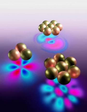 |
| Schematics of two types of optical circuits: the three particle trimer functions as a nanoscale magnet, while the seven particle heptamer exhibits almost no scattering for a narrow range of wavelengths due to interference. Credit: The laboratory of Federico Cappaso, Harvard School of Engineering and Applied Sciences |
Abstract:
Scalable devices inspired by nature exhibit customizable optical properties suitable for applications ranging from highly sensitive sensors and detectors to invisibility cloaks
Applied physicists create building blocks for a new class of optical circuits
Cambridge, MA | Posted on June 2nd, 2010Imagine creating novel devices with amazing and exotic optical properties not found in nature�by simply evaporating a droplet of particles on a surface.
By chemically building clusters of nanospheres from a liquid, a team of Harvard researchers, in collaboration with scientists at Rice University, the University of Texas at Austin, and the University of Houston, has developed just that.
The finding, published in the May 28 issue of Science, demonstrates simple scalable devices that exhibit customizable optical properties suitable for applications ranging from highly sensitive sensors and detectors to invisibility cloaks. Using particles consisting of concentric metallic and insulating shells, Jonathan Fan, a graduate student at the Harvard School of Engineering and Applied Sciences (SEAS), his lead co-author Federico Capasso, Robert L. Wallace Professor of Applied Physics and Vinton Hayes Senior Research Fellow in Electrical Engineering at SEAS, and Vinothan Manoharan, Associate professor of Chemical Engineering and Physics at SEAS and Harvard's Physics Department, devised a bottom-up, self-assembly approach to meet the design challenge.
"A longstanding challenge in optical engineering has been to find ways to make structures of size much smaller than the wavelength that exhibit desired and interesting properties," says Fan. "At visible frequencies, these structures must be nanoscale."
In contrast, most nanoscale devices are fabricated using top-down approaches, akin to how computer chips are manufactured. The smallest sizes that can be realized by such techniques are severely constrained by the intrinsic limits of the fabrication process, such as the wavelength of light used in the process. Moreover, such methods are restricted to planar geometries, are expensive, and require intense infrastructure such as cleanrooms.
"With our bottom-up approach, we mimic the way nature creates innovative structures, which exhibit extremely useful properties," explains Capasso. "Our nanoclusters behave as tiny optical circuits and could be the basis of new technology such as detectors of single molecules, efficient and biologically compatible probes in cancer therapeutics, and optical tweezers to manipulate and sort out nano-sized particles. Moreover, the fabrication process is much simpler and cheaper to carry out."
The researcher's self-assembly method requires nothing more than a bit of mixing and drying. To form the clusters, the particles are first coated with a polymer, and a droplet of them is then evaporated on a water-repellent surface. In the process of evaporation, the particles pack together into small clusters. Using polymer spacers to separate the nanoparticles, the researchers were able to controllably achieve a two nanometer gap between the particles�far better resolution than traditional top-down methods allow.
Two types of resulting optical circuits are of considerable interest. A trimer, comprising three equally-spaced particles, can support a magnetic response, an essential property of invisibility cloaks and materials that exhibit negative refractive index.
"In essence, the trimer acts as a nanoscale resonator that can support a circulating loop of current at visible and near-infrared frequencies," says Fan. "This structure functions as a nanoscale magnet at optical frequencies, something that natural materials cannot do."
Heptamers, or packed seven particle structures, exhibit almost no scattering for a narrow range of well-defined colors or wavelengths when illuminated with white light. These sharp dips, known as Fano resonances, arise from the interference of two modes of electron oscillations, a "bright" mode and a non-optically active "dark" mode, in the nanoparticle.
"Heptamers are very efficient at creating extremely intense electric fields localized in nanometer-size regions where molecules and nanoscale particles can be trapped, manipulated, and detected. Molecular sensing would rely on detecting shifts in the narrow spectra dips," says Capasso.
Ultimately, all of the self-assembled circuit designs can be readily tuned by varying the geometry, how the particles are separated, and the chemical environment. In short, the new method allows a "tool kit" for manipulating "artificial molecules" in such a way to create optical properties at will, a feature the researchers expect is broadly generalizable to a host of other characteristics.
Looking ahead, the researchers plan to work on achieving higher cluster yields and hope to assemble three-dimensional structures at the macroscale, a "holy grail" of materials science.
"We are excited by the potentially scalability of the method," says Manoharan. "Spheres are the easiest shapes to assemble as they can be readily packed together. While we only demonstrated here planar particle clusters, our method can be extended to three-dimensional structures, something that a top-down approach would have difficulty doing."
Fan, Capasso, and Manoharan's co-authors included Chihhui Wu and Gennady Shvets of University of Texas at Austin; Jiming Bao of the University of Houston; and Kui Bao, Rizia Bardhan, Naomi Halas, and Peter Norlander, all of Rice University.
The researchers acknowledge the support of National Science Foundation, the Air Force Office of Scientific Research; the U.S. Department of Defense; the Robert A. Welch Foundation; and the Center for Advanced Solar Photophysics, a U.S. Department of Energy Frontier Research Center. The work was carried out at the Center for Nanoscale Systems at Harvard, a member of the National Nanotechnology Infrastructure Network.
####
For more information, please click here
Contacts:
Michael Patrick Rutter
617-496-3815
Copyright © Harvard University
If you have a comment, please Contact us.Issuers of news releases, not 7th Wave, Inc. or Nanotechnology Now, are solely responsible for the accuracy of the content.
Bookmark:


| Related News Press |
News and information
![]() Quantum computer improves AI predictions April 17th, 2026
Quantum computer improves AI predictions April 17th, 2026
![]() Flexible sensor gains sensitivity under pressure April 17th, 2026
Flexible sensor gains sensitivity under pressure April 17th, 2026
![]() A reusable chip for particulate matter sensing April 17th, 2026
A reusable chip for particulate matter sensing April 17th, 2026
![]() Detecting vibrational quantum beating in the predissociation dynamics of SF6 using time-resolved photoelectron spectroscopy April 17th, 2026
Detecting vibrational quantum beating in the predissociation dynamics of SF6 using time-resolved photoelectron spectroscopy April 17th, 2026
Govt.-Legislation/Regulation/Funding/Policy
![]() Quantum computer improves AI predictions April 17th, 2026
Quantum computer improves AI predictions April 17th, 2026
![]() Metasurfaces smooth light to boost magnetic sensing precision January 30th, 2026
Metasurfaces smooth light to boost magnetic sensing precision January 30th, 2026
![]() New imaging approach transforms study of bacterial biofilms August 8th, 2025
New imaging approach transforms study of bacterial biofilms August 8th, 2025
Possible Futures
![]() A fundamentally new therapeutic approach to cystic fibrosis: Nanobody repairs cellular defect April 17th, 2026
A fundamentally new therapeutic approach to cystic fibrosis: Nanobody repairs cellular defect April 17th, 2026
![]() UC Irvine physicists discover method to reverse �quantum scrambling� : The work addresses the problem of information loss in quantum computing system April 17th, 2026
UC Irvine physicists discover method to reverse �quantum scrambling� : The work addresses the problem of information loss in quantum computing system April 17th, 2026
Academic/Education
![]() Rice University launches Rice Synthetic Biology Institute to improve lives January 12th, 2024
Rice University launches Rice Synthetic Biology Institute to improve lives January 12th, 2024
![]() Multi-institution, $4.6 million NSF grant to fund nanotechnology training September 9th, 2022
Multi-institution, $4.6 million NSF grant to fund nanotechnology training September 9th, 2022
Self Assembly
![]() Diamond glitter: A play of colors with artificial DNA crystals May 17th, 2024
Diamond glitter: A play of colors with artificial DNA crystals May 17th, 2024
![]() Liquid crystal templated chiral nanomaterials October 14th, 2022
Liquid crystal templated chiral nanomaterials October 14th, 2022
![]() Nanoclusters self-organize into centimeter-scale hierarchical assemblies April 22nd, 2022
Nanoclusters self-organize into centimeter-scale hierarchical assemblies April 22nd, 2022
![]() Atom by atom: building precise smaller nanoparticles with templates March 4th, 2022
Atom by atom: building precise smaller nanoparticles with templates March 4th, 2022
Nanomedicine
![]() A fundamentally new therapeutic approach to cystic fibrosis: Nanobody repairs cellular defect April 17th, 2026
A fundamentally new therapeutic approach to cystic fibrosis: Nanobody repairs cellular defect April 17th, 2026
![]() New molecular technology targets tumors and simultaneously silences two �undruggable� cancer genes August 8th, 2025
New molecular technology targets tumors and simultaneously silences two �undruggable� cancer genes August 8th, 2025
![]() New imaging approach transforms study of bacterial biofilms August 8th, 2025
New imaging approach transforms study of bacterial biofilms August 8th, 2025
![]() Electrifying results shed light on graphene foam as a potential material for lab grown cartilage June 6th, 2025
Electrifying results shed light on graphene foam as a potential material for lab grown cartilage June 6th, 2025
Sensors
![]() Flexible sensor gains sensitivity under pressure April 17th, 2026
Flexible sensor gains sensitivity under pressure April 17th, 2026
![]() Tiny nanosheets, big leap: A new sensor detects ethanol at ultra-low levels January 30th, 2026
Tiny nanosheets, big leap: A new sensor detects ethanol at ultra-low levels January 30th, 2026
![]() From sensors to smart systems: the rise of AI-driven photonic noses January 30th, 2026
From sensors to smart systems: the rise of AI-driven photonic noses January 30th, 2026
![]() Sensors innovations for smart lithium-based batteries: advancements, opportunities, and potential challenges August 8th, 2025
Sensors innovations for smart lithium-based batteries: advancements, opportunities, and potential challenges August 8th, 2025
Announcements
![]() A fundamentally new therapeutic approach to cystic fibrosis: Nanobody repairs cellular defect April 17th, 2026
A fundamentally new therapeutic approach to cystic fibrosis: Nanobody repairs cellular defect April 17th, 2026
![]() UC Irvine physicists discover method to reverse �quantum scrambling� : The work addresses the problem of information loss in quantum computing system April 17th, 2026
UC Irvine physicists discover method to reverse �quantum scrambling� : The work addresses the problem of information loss in quantum computing system April 17th, 2026
Tools
![]() Metasurfaces smooth light to boost magnetic sensing precision January 30th, 2026
Metasurfaces smooth light to boost magnetic sensing precision January 30th, 2026
![]() From sensors to smart systems: the rise of AI-driven photonic noses January 30th, 2026
From sensors to smart systems: the rise of AI-driven photonic noses January 30th, 2026
![]() Japan launches fully domestically produced quantum computer: Expo visitors to experience quantum computing firsthand August 8th, 2025
Japan launches fully domestically produced quantum computer: Expo visitors to experience quantum computing firsthand August 8th, 2025
Photonics/Optics/Lasers
![]() Metasurfaces smooth light to boost magnetic sensing precision January 30th, 2026
Metasurfaces smooth light to boost magnetic sensing precision January 30th, 2026
![]() From sensors to smart systems: the rise of AI-driven photonic noses January 30th, 2026
From sensors to smart systems: the rise of AI-driven photonic noses January 30th, 2026
Research partnerships
![]() Lab to industry: InSe wafer-scale breakthrough for future electronics August 8th, 2025
Lab to industry: InSe wafer-scale breakthrough for future electronics August 8th, 2025
![]() HKU physicists uncover hidden order in the quantum world through deconfined quantum critical points April 25th, 2025
HKU physicists uncover hidden order in the quantum world through deconfined quantum critical points April 25th, 2025
|
|
||
|
|
||
| The latest news from around the world, FREE | ||
|
|
||
|
|
||
| Premium Products | ||
|
|
||
|
Only the news you want to read!
Learn More |
||
|
|
||
|
Full-service, expert consulting
Learn More |
||
|
|
||