Home > Press > Silicon Integrated Nanophotonics
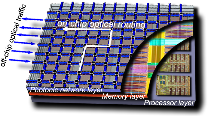 |
| Artist� concept of 3D silicon processor chip with optical IO layer featuring on-chip nanophotonic network. Courtesy IBM. |
Abstract:
Development of on-chip optical interconnects for future multi-core processors
Silicon Integrated Nanophotonics
Yorktown Heights, NY | Posted on March 6th, 2010The ultimate goal of this project is to develop a technology for on-chip integration of ultra-compact nanophotonic circuits for manipulating the light signals, similar to the way electrical signals are manipulated in computer chips. Nanoscale silicon photonics circuits are being developed to enable the integration of complete optical systems on a monolithic semiconductor chip that would eventually allow to overcome severe constraints of today's mostly copper I/O interconnects.
The current tendency in high performance computing systems is to increase the parallelism in processing at all levels utilizing multithreads, increasing the number of chips in racks and blades, as well as increasing the number of cores on a chip. The scaling of overall system performance that soon might approach Exaflop/s is, however, out of balance with respect to limited available bandwidth for shuttling ExaBytes of data across the system, between the racks, chips and cores.
Optics is destined to be utilized in data centers since optical communications can meet the large bandwidth demands of high-performance computing systems by bringing the immense advantages of high modulation rates and parallelism of wavelength division multiplexing. As it already happened in long-haul communications decades ago when optical fibers replaced copper cables, the copper cables that connect racks in the datacenters are started now to being replaced by optical fibers. Following the same trend optics can become competitive with copper at shorter and shorter distances eventually leading to optical on-board and may be even on-chip communications.
This future 3D-integated chip consists of several layers connected with each other with very dense and small pitch interlayer vias. The lower layer is a processor itself with many hundreds of individual cores. Memory layer (or layers) are bonded on top to provide fast access to local caches. On top of the stack is the Photonic layer with many thousands of individual optical devices (modulators, detectors, switches) as well as analogue electrical circuits (amplifiers, drivers, latches, etc.). The key role of a photonic layer is not only to provide point-to-point broad bandwidth optical link between different cores and/or the off-chip traffic, but also to route this traffic with an array of nanophotonic switches. Hence it is named Intra-chip optical network (ICON).
Silicon photonics offers high density integration of individual optical components on a single chip. Strong light confinement enables dramatic scaling of the device area and allows unprecedented control over optical signals. Silicon nanophotonic devices have immense capacity for low-loss, high-bandwidth data processing. Fabrication of silicon photonics system in the complementary metal-oxide-semiconductor (CMOS)-compatible silicon-on-insulator platform also results in further integration of optical and electrical circuitry. Following the Moore's scaling laws in electronics, dense chip-scale integration of optical components can bring the price and power per a bit of transferred data low enough to enable optical communications in high performance computing systems.
To meet these stringent requirements and utilize fully all the benefits of optics an innovative engineering is necessary at all levels starting from the design of individual devices to the overall architecture of high-performance computing system. Nanoscale silicon photonics circuits that are being developed within this project are targeted to enable the monolithic integration of complete optical systems on a semiconductor chip.
More: www.research.ibm.com/photonics/publications/ecoc_tutorial_2008.pdf
####
For more information, please click here
Contacts:
Main operator
(914) 945-3000
Copyright © IBM
If you have a comment, please Contact us.Issuers of news releases, not 7th Wave, Inc. or Nanotechnology Now, are solely responsible for the accuracy of the content.
Bookmark:


| Related News Press |
News and information
![]() Quantum computer improves AI predictions April 17th, 2026
Quantum computer improves AI predictions April 17th, 2026
![]() Flexible sensor gains sensitivity under pressure April 17th, 2026
Flexible sensor gains sensitivity under pressure April 17th, 2026
![]() A reusable chip for particulate matter sensing April 17th, 2026
A reusable chip for particulate matter sensing April 17th, 2026
![]() Detecting vibrational quantum beating in the predissociation dynamics of SF6 using time-resolved photoelectron spectroscopy April 17th, 2026
Detecting vibrational quantum beating in the predissociation dynamics of SF6 using time-resolved photoelectron spectroscopy April 17th, 2026
Possible Futures
![]() A fundamentally new therapeutic approach to cystic fibrosis: Nanobody repairs cellular defect April 17th, 2026
A fundamentally new therapeutic approach to cystic fibrosis: Nanobody repairs cellular defect April 17th, 2026
![]() UC Irvine physicists discover method to reverse �quantum scrambling� : The work addresses the problem of information loss in quantum computing system April 17th, 2026
UC Irvine physicists discover method to reverse �quantum scrambling� : The work addresses the problem of information loss in quantum computing system April 17th, 2026
Chip Technology
![]() A reusable chip for particulate matter sensing April 17th, 2026
A reusable chip for particulate matter sensing April 17th, 2026
![]() Metasurfaces smooth light to boost magnetic sensing precision January 30th, 2026
Metasurfaces smooth light to boost magnetic sensing precision January 30th, 2026
Nanoelectronics
![]() Lab to industry: InSe wafer-scale breakthrough for future electronics August 8th, 2025
Lab to industry: InSe wafer-scale breakthrough for future electronics August 8th, 2025
![]() Interdisciplinary: Rice team tackles the future of semiconductors Multiferroics could be the key to ultralow-energy computing October 6th, 2023
Interdisciplinary: Rice team tackles the future of semiconductors Multiferroics could be the key to ultralow-energy computing October 6th, 2023
![]() Key element for a scalable quantum computer: Physicists from Forschungszentrum J�lich and RWTH Aachen University demonstrate electron transport on a quantum chip September 23rd, 2022
Key element for a scalable quantum computer: Physicists from Forschungszentrum J�lich and RWTH Aachen University demonstrate electron transport on a quantum chip September 23rd, 2022
![]() Reduced power consumption in semiconductor devices September 23rd, 2022
Reduced power consumption in semiconductor devices September 23rd, 2022
Announcements
![]() A fundamentally new therapeutic approach to cystic fibrosis: Nanobody repairs cellular defect April 17th, 2026
A fundamentally new therapeutic approach to cystic fibrosis: Nanobody repairs cellular defect April 17th, 2026
![]() UC Irvine physicists discover method to reverse �quantum scrambling� : The work addresses the problem of information loss in quantum computing system April 17th, 2026
UC Irvine physicists discover method to reverse �quantum scrambling� : The work addresses the problem of information loss in quantum computing system April 17th, 2026
Photonics/Optics/Lasers
![]() Metasurfaces smooth light to boost magnetic sensing precision January 30th, 2026
Metasurfaces smooth light to boost magnetic sensing precision January 30th, 2026
![]() From sensors to smart systems: the rise of AI-driven photonic noses January 30th, 2026
From sensors to smart systems: the rise of AI-driven photonic noses January 30th, 2026
|
|
||
|
|
||
| The latest news from around the world, FREE | ||
|
|
||
|
|
||
| Premium Products | ||
|
|
||
|
Only the news you want to read!
Learn More |
||
|
|
||
|
Full-service, expert consulting
Learn More |
||
|
|
||