Home > Press > Digging deep into diamonds
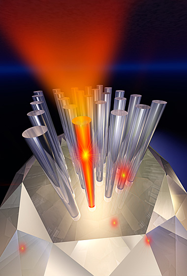 |
| Researchers used a top-down nanofabrication technique to embed color centers into a variety of machined structures. By creating large device arrays rather than just "one-of-a-kind" designs, the realization of quantum networks and systems, which require the integration and manipulation of many devices in parallel, is more likely. Illustration by Jay Penni. |
Abstract:
Diamond-based nanowire devices advance quantum science
Digging deep into diamonds
Cambridge, MA | Posted on February 15th, 2010By creating diamond-based nanowire devices, a team at Harvard University has taken another step toward making applications based on quantum science and technology possible.
The new device offers a bright, stable source of single photons at room temperature, an essential element in making fast and secure computing with light practical.
The finding could lead to a new class of nanostructured diamond devices suitable for quantum communication and computing, as well as advance areas ranging from biological and chemical sensing to scientific imaging.
Published in the Feb. 14 issue of Nature Nanotechnology, researchers led by Marko Loncar, assistant professor of electrical engineering at Harvard's School of Engineering and Applied Sciences (SEAS), found that the performance of a single photon source based on a light-emitting defect (color center) in a diamond could be improved by nanostructuring the diamond and embedding the defect within a diamond nanowire.
Scientists, in fact, first began exploiting the properties of natural diamonds after learning how to manipulate the electron spin, or intrinsic angular momentum, associated with the nitrogen vacancy (NV) color center of the gem. The quantum (qubit) state can be initialized and measured using light.
The color center "communicates" by emitting and absorbing photons. The flow of photons emitted from the color center provides a means to carry the resulting information, making the control, capture, and storage of photons essential for any kind of practical communication or computation. Gathering photons efficiently, however, is difficult since color centers are embedded deep inside the diamond.
"This presents a major problem if you want to interface a color center and integrate it into real-world applications," explains Loncar. "What was missing was an interface that connects the nano-world of a color center with the macro-world of optical fibers and lenses."
The diamond nanowire device offers a solution, providing a natural and efficient interface to probe an individual color center, making it brighter and increasing its sensitivity. The resulting enhanced optical properties increase photon collection by nearly a factor of ten relative to natural diamond devices.
"Our nanowire device can channel the photons that are emitted and direct them in a convenient way," says lead author Thomas Babinec, a graduate student at SEAS.
Further, the diamond nanowire is designed to overcome hurdles that have challenged other state-of-the-art systems � such as those based on fluorescent dye molecules, quantum dots, and carbon nanotubes � as the device can be readily replicated and integrated with a variety of nano-machined structures.
The researchers used a top-down nanofabrication technique to embed color centers into a variety of machined structures. By creating large device arrays rather than just "one-of-a-kind" designs, the realization of quantum networks and systems, which require the integration and manipulation of many devices in parallel, is more likely.
"We consider this an important step in enabling technology towards more practical optical systems based on this exciting material platform," says Loncar. "Starting with these synthetic, nanostructured diamond samples, we can start dreaming about the diamond-based devices and systems that could one day lead to applications in quantum science and technology as well as in sensing and imaging."
Loncar and Babinec's co-authors included research scholar Birgit Hausmann, graduate student Yinan Zhang, and postdoctoral student Mughees Khan, all at SEAS; graduate student Jero Maze in the Department of Physics at Harvard; and faculty member Phil R. Hemmer at Texas A&M University.
The researchers acknowledge the following support: Nanoscale Interdisciplinary Research Team (NIRT) grant from National Science Foundation (NSF), the NSF-funded Nanoscale Science and Engineering Center at Harvard (NSEC); the Defense Advanced Research Projects Agency (DARPA); and a National Defense Science and Engineering Graduate Fellowship and NSF Graduate Fellowship. All devices have been fabricated at the Center for Nanoscale Systems (CNS) at Harvard.
####
About Harvard University
Harvard University is made up of 11 principal academic units � ten faculties and the Radcliffe Institute for Advanced Study. The ten faculties oversee schools and divisions that offer courses and award academic degrees.
For more information, please click here
Copyright © Harvard University
If you have a comment, please Contact us.Issuers of news releases, not 7th Wave, Inc. or Nanotechnology Now, are solely responsible for the accuracy of the content.
Bookmark:


| Related News Press |
News and information
![]() Quantum computer improves AI predictions April 17th, 2026
Quantum computer improves AI predictions April 17th, 2026
![]() Flexible sensor gains sensitivity under pressure April 17th, 2026
Flexible sensor gains sensitivity under pressure April 17th, 2026
![]() A reusable chip for particulate matter sensing April 17th, 2026
A reusable chip for particulate matter sensing April 17th, 2026
![]() Detecting vibrational quantum beating in the predissociation dynamics of SF6 using time-resolved photoelectron spectroscopy April 17th, 2026
Detecting vibrational quantum beating in the predissociation dynamics of SF6 using time-resolved photoelectron spectroscopy April 17th, 2026
Govt.-Legislation/Regulation/Funding/Policy
![]() Quantum computer improves AI predictions April 17th, 2026
Quantum computer improves AI predictions April 17th, 2026
![]() Metasurfaces smooth light to boost magnetic sensing precision January 30th, 2026
Metasurfaces smooth light to boost magnetic sensing precision January 30th, 2026
![]() New imaging approach transforms study of bacterial biofilms August 8th, 2025
New imaging approach transforms study of bacterial biofilms August 8th, 2025
Possible Futures
![]() A fundamentally new therapeutic approach to cystic fibrosis: Nanobody repairs cellular defect April 17th, 2026
A fundamentally new therapeutic approach to cystic fibrosis: Nanobody repairs cellular defect April 17th, 2026
![]() UC Irvine physicists discover method to reverse �quantum scrambling� : The work addresses the problem of information loss in quantum computing system April 17th, 2026
UC Irvine physicists discover method to reverse �quantum scrambling� : The work addresses the problem of information loss in quantum computing system April 17th, 2026
Nanotubes/Buckyballs/Fullerenes/Nanorods/Nanostrings/Nanosheets
![]() Tiny nanosheets, big leap: A new sensor detects ethanol at ultra-low levels January 30th, 2026
Tiny nanosheets, big leap: A new sensor detects ethanol at ultra-low levels January 30th, 2026
![]() Enhancing power factor of p- and n-type single-walled carbon nanotubes April 25th, 2025
Enhancing power factor of p- and n-type single-walled carbon nanotubes April 25th, 2025
![]() Chainmail-like material could be the future of armor: First 2D mechanically interlocked polymer exhibits exceptional flexibility and strength January 17th, 2025
Chainmail-like material could be the future of armor: First 2D mechanically interlocked polymer exhibits exceptional flexibility and strength January 17th, 2025
![]() Innovative biomimetic superhydrophobic coating combines repair and buffering properties for superior anti-erosion December 13th, 2024
Innovative biomimetic superhydrophobic coating combines repair and buffering properties for superior anti-erosion December 13th, 2024
Quantum Computing
![]() Quantum computer improves AI predictions April 17th, 2026
Quantum computer improves AI predictions April 17th, 2026
![]() UC Irvine physicists discover method to reverse �quantum scrambling� : The work addresses the problem of information loss in quantum computing system April 17th, 2026
UC Irvine physicists discover method to reverse �quantum scrambling� : The work addresses the problem of information loss in quantum computing system April 17th, 2026
![]() Researchers develop molecular qubits that communicate at telecom frequencies October 3rd, 2025
Researchers develop molecular qubits that communicate at telecom frequencies October 3rd, 2025
Sensors
![]() Flexible sensor gains sensitivity under pressure April 17th, 2026
Flexible sensor gains sensitivity under pressure April 17th, 2026
![]() Tiny nanosheets, big leap: A new sensor detects ethanol at ultra-low levels January 30th, 2026
Tiny nanosheets, big leap: A new sensor detects ethanol at ultra-low levels January 30th, 2026
![]() From sensors to smart systems: the rise of AI-driven photonic noses January 30th, 2026
From sensors to smart systems: the rise of AI-driven photonic noses January 30th, 2026
![]() Sensors innovations for smart lithium-based batteries: advancements, opportunities, and potential challenges August 8th, 2025
Sensors innovations for smart lithium-based batteries: advancements, opportunities, and potential challenges August 8th, 2025
Announcements
![]() A fundamentally new therapeutic approach to cystic fibrosis: Nanobody repairs cellular defect April 17th, 2026
A fundamentally new therapeutic approach to cystic fibrosis: Nanobody repairs cellular defect April 17th, 2026
![]() UC Irvine physicists discover method to reverse �quantum scrambling� : The work addresses the problem of information loss in quantum computing system April 17th, 2026
UC Irvine physicists discover method to reverse �quantum scrambling� : The work addresses the problem of information loss in quantum computing system April 17th, 2026
Quantum Dots/Rods
![]() A new kind of magnetism November 17th, 2023
A new kind of magnetism November 17th, 2023
![]() IOP Publishing celebrates World Quantum Day with the announcement of a special quantum collection and the winners of two prestigious quantum awards April 14th, 2023
IOP Publishing celebrates World Quantum Day with the announcement of a special quantum collection and the winners of two prestigious quantum awards April 14th, 2023
![]() Qubits on strong stimulants: Researchers find ways to improve the storage time of quantum information in a spin rich material January 27th, 2023
Qubits on strong stimulants: Researchers find ways to improve the storage time of quantum information in a spin rich material January 27th, 2023
![]() NIST�s grid of quantum islands could reveal secrets for powerful technologies November 18th, 2022
NIST�s grid of quantum islands could reveal secrets for powerful technologies November 18th, 2022
Alliances/Trade associations/Partnerships/Distributorships
![]() Chicago Quantum Exchange welcomes six new partners highlighting quantum technology solutions, from Chicago and beyond September 23rd, 2022
Chicago Quantum Exchange welcomes six new partners highlighting quantum technology solutions, from Chicago and beyond September 23rd, 2022
![]() University of Illinois Chicago joins Brookhaven Lab's Quantum Center June 10th, 2022
University of Illinois Chicago joins Brookhaven Lab's Quantum Center June 10th, 2022
Quantum nanoscience
![]() Beyond silicon: Electronics at the scale of a single molecule January 30th, 2026
Beyond silicon: Electronics at the scale of a single molecule January 30th, 2026
![]() MXene nanomaterials enter a new dimension Multilayer nanomaterial: MXene flakes created at Drexel University show new promise as 1D scrolls January 30th, 2026
MXene nanomaterials enter a new dimension Multilayer nanomaterial: MXene flakes created at Drexel University show new promise as 1D scrolls January 30th, 2026
![]() ICFO researchers overcome long-standing bottleneck in single photon detection with twisted 2D materials August 8th, 2025
ICFO researchers overcome long-standing bottleneck in single photon detection with twisted 2D materials August 8th, 2025
|
|
||
|
|
||
| The latest news from around the world, FREE | ||
|
|
||
|
|
||
| Premium Products | ||
|
|
||
|
Only the news you want to read!
Learn More |
||
|
|
||
|
Full-service, expert consulting
Learn More |
||
|
|
||