Home > Press > Contact lens with integrated inorganic semiconductor device
 |
Abstract:
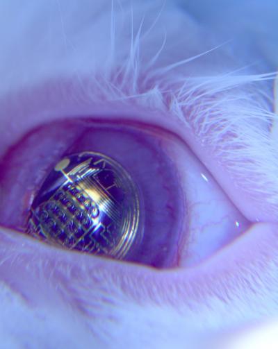
Conventional contact lenses are simple polymer structures primarily used for the correction of vision. The integration of function into the structure of a contact lens opens a number of intriguing venues such as incorporation of a semi-transparent display directly on the structure of a contact lens or the inclusion of a bio-sensor directly on the surface of the cornea. Contact lens have been tested and used biocompatible for use in a rabbit eye [1].
Contact lens with integrated inorganic semiconductor device
Napoli, Italy | Posted on August 24th, 2009After the experiment we are try to install the electronic circuit on a contact lens for use human. The integration on contact lens with embedded electronics, optoelectronics, or sensors, in addition to vision correction, can act as a head-up display (HUD) or a medical sensing instrument. Automakers have begun incorporating HUDs into their cars for the purpose of displaying data such as vehicle speed directly onto the windshield. The idea is to create a safer driving experience by allowing the driver to stay focused on the road while having all pertinent information directly in his field of vision [1].
All HUD systems in use today require sizeable pieces of equipment that are not very portable and infringe on the user's mobility. By placing portions of a HUD system onto a contact lens, and precisely LED (light emitting diode) display, on the contact lens, it is possible to create a system that is compact, portable, and discrete.
The same benefits can be realized when using the contact lens as a medical instrument. Glucose sensors for example, among other sensors, can be placed onto the contact to provide early warnings to diabetics.
Contact lens with integrate display can give information of the viability, by HUD's, to the driver.
Video-game companies could use the contact lenses to completely immerse players in a virtual world without restricting their range of motion [1]. We offer a set of technique based on self-assembly here that allow for incorporation of various functions onto a contact lens.
Contact lens is made of polyethylene terephthalate (PET) that is a thermoplastic polymeric resin used for synthetic fibre, member of the family of polyesters that are a class of polymers that contained a ester group in their main chain.
Such an integrated device would presently have a wide range of uses for biological and chemical analysis and may open doors for new applications in the future. Final platform is composted of unconventional substrate utilizing simply fabrication technique and common materials such as plastic or glass used to fluorescence detection that is the primary method of molecular sensing and characterization in biology today.
After the self-assembly process, the surface is encapsulated with a biocompatible material, polymethyl methacrylate (PMMA). Once passivated, the flat substrate with embedded electronics is placed into a heated aluminum mold and pressed so that a permanent curvature is imparted onto the plastic creating the contact lens. The lens is then sterilized and tested in a rabbit's eye that represent animal model of this experiment.
Bibliography
[1] Contact lens with integrated inorganic
semiconductor devices Ho, H. Saeedi, E. Kim,
S.S.Shen, T.T. Parviz, B.A.
Micro Electro Mechanical Systems
IEEE 21st International Conference on 403-406 Jan. 2008
[2] S.A. Stauth, B.A. Parviz, "Self-assembled singlecrystal
silicon circuits on plastic", Proceedings of the
National Academy of Sciences, vol. 103, pp. 13922-
13927, 2006.
[3] S.S. Kim, E. Saeedi, D.R. Meldrum, B.A. Parviz, "Self-
Assembled Heterogeneous Integrated Fluorescence
Detection System", proceedings of the 2nd Annual
IEEE International Conference on Nano/Micro
Engineered and Molecular Systems, pp. 927-931, 2007.
[4] B. Monemar, K.K. Shih, G.D. Pettit, "Some optical
properties of the AlxGa1-xAs alloy system", Journal of
applied physics, vol.47, no.6, 1976.
[5] X. Wu, L. Coldren, J. Merz, "Selectrive etching
characteristics of HF for AlxGa1-xAs," Electronics
Letters, vol. 21, pp 558-559, 1985.
[6] Ehsan Saeedi1*, Samuel S. Kim1, James R. Etzkorn,
Dierdre R. Meldrum2, Fellow, IEEE, and Babak A. Parviz1
Automation and yield of micron-scale self-assembly processes
IEEE Conference on Automation Science and Engineering
Scottsdale, AZ, USA, Sept 22-25, pp. 375-380, 2007.
Dott. Giovanni Romano
University Federico II Naples Italy
####
For more information, please click here
Contacts:
Giovanni Romano
Phone: 3478389514
or
Copyright © Univ. Federico II
If you have a comment, please Contact us.Issuers of news releases, not 7th Wave, Inc. or Nanotechnology Now, are solely responsible for the accuracy of the content.
Bookmark:


| Related News Press |
News and information
![]() Quantum computer improves AI predictions April 17th, 2026
Quantum computer improves AI predictions April 17th, 2026
![]() Flexible sensor gains sensitivity under pressure April 17th, 2026
Flexible sensor gains sensitivity under pressure April 17th, 2026
![]() A reusable chip for particulate matter sensing April 17th, 2026
A reusable chip for particulate matter sensing April 17th, 2026
![]() Detecting vibrational quantum beating in the predissociation dynamics of SF6 using time-resolved photoelectron spectroscopy April 17th, 2026
Detecting vibrational quantum beating in the predissociation dynamics of SF6 using time-resolved photoelectron spectroscopy April 17th, 2026
Display technology/LEDs/SS Lighting/OLEDs
![]() Spinel-type sulfide semiconductors to operate the next-generation LEDs and solar cells For solar-cell absorbers and green-LED source October 3rd, 2025
Spinel-type sulfide semiconductors to operate the next-generation LEDs and solar cells For solar-cell absorbers and green-LED source October 3rd, 2025
![]() Efficient and stable hybrid perovskite-organic light-emitting diodes with external quantum efficiency exceeding 40 per cent July 5th, 2024
Efficient and stable hybrid perovskite-organic light-emitting diodes with external quantum efficiency exceeding 40 per cent July 5th, 2024
Nanomedicine
![]() A fundamentally new therapeutic approach to cystic fibrosis: Nanobody repairs cellular defect April 17th, 2026
A fundamentally new therapeutic approach to cystic fibrosis: Nanobody repairs cellular defect April 17th, 2026
![]() New molecular technology targets tumors and simultaneously silences two �undruggable� cancer genes August 8th, 2025
New molecular technology targets tumors and simultaneously silences two �undruggable� cancer genes August 8th, 2025
![]() New imaging approach transforms study of bacterial biofilms August 8th, 2025
New imaging approach transforms study of bacterial biofilms August 8th, 2025
![]() Electrifying results shed light on graphene foam as a potential material for lab grown cartilage June 6th, 2025
Electrifying results shed light on graphene foam as a potential material for lab grown cartilage June 6th, 2025
Sensors
![]() Flexible sensor gains sensitivity under pressure April 17th, 2026
Flexible sensor gains sensitivity under pressure April 17th, 2026
![]() Tiny nanosheets, big leap: A new sensor detects ethanol at ultra-low levels January 30th, 2026
Tiny nanosheets, big leap: A new sensor detects ethanol at ultra-low levels January 30th, 2026
![]() From sensors to smart systems: the rise of AI-driven photonic noses January 30th, 2026
From sensors to smart systems: the rise of AI-driven photonic noses January 30th, 2026
![]() Sensors innovations for smart lithium-based batteries: advancements, opportunities, and potential challenges August 8th, 2025
Sensors innovations for smart lithium-based batteries: advancements, opportunities, and potential challenges August 8th, 2025
Discoveries
![]() Quantum computer improves AI predictions April 17th, 2026
Quantum computer improves AI predictions April 17th, 2026
![]() Flexible sensor gains sensitivity under pressure April 17th, 2026
Flexible sensor gains sensitivity under pressure April 17th, 2026
![]() A reusable chip for particulate matter sensing April 17th, 2026
A reusable chip for particulate matter sensing April 17th, 2026
![]() Detecting vibrational quantum beating in the predissociation dynamics of SF6 using time-resolved photoelectron spectroscopy April 17th, 2026
Detecting vibrational quantum beating in the predissociation dynamics of SF6 using time-resolved photoelectron spectroscopy April 17th, 2026
Announcements
![]() A fundamentally new therapeutic approach to cystic fibrosis: Nanobody repairs cellular defect April 17th, 2026
A fundamentally new therapeutic approach to cystic fibrosis: Nanobody repairs cellular defect April 17th, 2026
![]() UC Irvine physicists discover method to reverse �quantum scrambling� : The work addresses the problem of information loss in quantum computing system April 17th, 2026
UC Irvine physicists discover method to reverse �quantum scrambling� : The work addresses the problem of information loss in quantum computing system April 17th, 2026
|
|
||
|
|
||
| The latest news from around the world, FREE | ||
|
|
||
|
|
||
| Premium Products | ||
|
|
||
|
Only the news you want to read!
Learn More |
||
|
|
||
|
Full-service, expert consulting
Learn More |
||
|
|
||