Home > Press > Scientists develop world’s smallest diamond transistor
 |
Abstract:
Scientists at the University of Glasgow have developed the world's smallest diamond transistor.
At just 50 nanometres in length the ‘gate' of the diamond transistor developed by Dr David Moran, of the Department of Electronics & Electrical Engineering, is more than 1000 times smaller than the thickness of a human hair, and is half the size of the previous smallest diamond transistor developed by Japanese firm NTT.
Scientists develop world’s smallest diamond transistor
Glasgow, UK | Posted on April 17th, 2009Diamond is heralded as being an ideal material for the next generation of nanoscale electronic devices due to its amazing and unique properties and could help scientists develop nascent technologies such as Terahertz Imaging and Automotive Collision Detection.
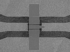
The ‘gate' of a transistor is used to control the flow of current between two electrical contact points, acting as a switch or an amplifier. The smaller the gate, the faster the transistor works.
Dr Moran said: "From its invention in 1947, the transistor has been the building block of many modern day technologies, from silicon based chips in your computer processor, to gallium arsenide based circuits in your mobile phone. The gate of the transistor (the section in the middle) developed by Dr Moran is just 50 nanometres in length.
"These types of materials - silicon and gallium arsenide - are chosen upon what their strengths and weaknesses are. Diamond on the other hand is very much an excellent all-round performer, and has been described by many as a perfect material.
"By developing a diamond transistor technology, we aim to tap into the truly amazing properties of this exciting material which could prove fundamental to the development of several next generation technologies."
Such technologies include Terahertz Imaging and Automotive Collision Detection.
Terahertz imaging uses terahertz radiation (T-rays) - electromagnetic waves of a frequency range between that of microwaves and infrared which can penetrate a range of materials, including clothes and flesh - to create a picture.
Because it is non-ionising, it does not damage cells and has potential applications in
security scanners to detect concealed weapons through clothes as well as safer medical imaging.
Automotive collision detection or automotive radar is an advanced safety feature currently being heavily researched by the car industry with which a car or other automotive vehicle will have an effective radar zone around it that will allow it to detect potential collisions from any side of the vehicle well in advance and take avoiding action.
Dr Moran added: "These applications require a very fast and ideally high-power transistor technology that needs to be able to operate in adverse weather/temperature conditions. This is where a diamond transistor technology would excel".
The diamond itself is artificially made by UK firm Element 6 through a process called chemical vapour deposition.
The creation of the tiny device is part of a five-year project funded by the Engineering & Physical Sciences Research Council (EPSRC) and is the result of a collaborative project between the University of Glasgow and Heriot Watt University. Its construction was only possible through the multi-million pound facilities within the James Watt Nanofabrication Centre at the University of Glasgow where electron beam lithography was employed to create patterns and structures on the miniscule sliver of diamond.
The University of Glasgow has one of the most advanced large area high-resolution electron beam lithography tools in the world.
####
For more information, please click here
Contacts:
Stuart Forsyth
University of Glasgow
Media Relations Office
44 0141 330 4831
Copyright © University of Glasgow
If you have a comment, please Contact us.Issuers of news releases, not 7th Wave, Inc. or Nanotechnology Now, are solely responsible for the accuracy of the content.
Bookmark:


| Related News Press |
News and information
![]() Quantum computer improves AI predictions April 17th, 2026
Quantum computer improves AI predictions April 17th, 2026
![]() Flexible sensor gains sensitivity under pressure April 17th, 2026
Flexible sensor gains sensitivity under pressure April 17th, 2026
![]() A reusable chip for particulate matter sensing April 17th, 2026
A reusable chip for particulate matter sensing April 17th, 2026
![]() Detecting vibrational quantum beating in the predissociation dynamics of SF6 using time-resolved photoelectron spectroscopy April 17th, 2026
Detecting vibrational quantum beating in the predissociation dynamics of SF6 using time-resolved photoelectron spectroscopy April 17th, 2026
Imaging
![]() Simple algorithm paired with standard imaging tool could predict failure in lithium metal batteries August 8th, 2025
Simple algorithm paired with standard imaging tool could predict failure in lithium metal batteries August 8th, 2025
Chip Technology
![]() A reusable chip for particulate matter sensing April 17th, 2026
A reusable chip for particulate matter sensing April 17th, 2026
![]() Metasurfaces smooth light to boost magnetic sensing precision January 30th, 2026
Metasurfaces smooth light to boost magnetic sensing precision January 30th, 2026
Nanoelectronics
![]() Lab to industry: InSe wafer-scale breakthrough for future electronics August 8th, 2025
Lab to industry: InSe wafer-scale breakthrough for future electronics August 8th, 2025
![]() Interdisciplinary: Rice team tackles the future of semiconductors Multiferroics could be the key to ultralow-energy computing October 6th, 2023
Interdisciplinary: Rice team tackles the future of semiconductors Multiferroics could be the key to ultralow-energy computing October 6th, 2023
![]() Key element for a scalable quantum computer: Physicists from Forschungszentrum Jülich and RWTH Aachen University demonstrate electron transport on a quantum chip September 23rd, 2022
Key element for a scalable quantum computer: Physicists from Forschungszentrum Jülich and RWTH Aachen University demonstrate electron transport on a quantum chip September 23rd, 2022
![]() Reduced power consumption in semiconductor devices September 23rd, 2022
Reduced power consumption in semiconductor devices September 23rd, 2022
Discoveries
![]() Quantum computer improves AI predictions April 17th, 2026
Quantum computer improves AI predictions April 17th, 2026
![]() Flexible sensor gains sensitivity under pressure April 17th, 2026
Flexible sensor gains sensitivity under pressure April 17th, 2026
![]() A reusable chip for particulate matter sensing April 17th, 2026
A reusable chip for particulate matter sensing April 17th, 2026
![]() Detecting vibrational quantum beating in the predissociation dynamics of SF6 using time-resolved photoelectron spectroscopy April 17th, 2026
Detecting vibrational quantum beating in the predissociation dynamics of SF6 using time-resolved photoelectron spectroscopy April 17th, 2026
Announcements
![]() A fundamentally new therapeutic approach to cystic fibrosis: Nanobody repairs cellular defect April 17th, 2026
A fundamentally new therapeutic approach to cystic fibrosis: Nanobody repairs cellular defect April 17th, 2026
![]() UC Irvine physicists discover method to reverse ‘quantum scrambling’ : The work addresses the problem of information loss in quantum computing system April 17th, 2026
UC Irvine physicists discover method to reverse ‘quantum scrambling’ : The work addresses the problem of information loss in quantum computing system April 17th, 2026
Tools
![]() Metasurfaces smooth light to boost magnetic sensing precision January 30th, 2026
Metasurfaces smooth light to boost magnetic sensing precision January 30th, 2026
![]() From sensors to smart systems: the rise of AI-driven photonic noses January 30th, 2026
From sensors to smart systems: the rise of AI-driven photonic noses January 30th, 2026
![]() Japan launches fully domestically produced quantum computer: Expo visitors to experience quantum computing firsthand August 8th, 2025
Japan launches fully domestically produced quantum computer: Expo visitors to experience quantum computing firsthand August 8th, 2025
Automotive/Transportation
![]() Decoding hydrogen‑bond network of electrolyte for cryogenic durable aqueous zinc‑ion batteries January 30th, 2026
Decoding hydrogen‑bond network of electrolyte for cryogenic durable aqueous zinc‑ion batteries January 30th, 2026
![]() Sensors innovations for smart lithium-based batteries: advancements, opportunities, and potential challenges August 8th, 2025
Sensors innovations for smart lithium-based batteries: advancements, opportunities, and potential challenges August 8th, 2025
![]() Simple algorithm paired with standard imaging tool could predict failure in lithium metal batteries August 8th, 2025
Simple algorithm paired with standard imaging tool could predict failure in lithium metal batteries August 8th, 2025
Printing/Lithography/Inkjet/Inks/Bio-printing/Dyes
![]() Presenting: Ultrasound-based printing of 3D materials—potentially inside the body December 8th, 2023
Presenting: Ultrasound-based printing of 3D materials—potentially inside the body December 8th, 2023
![]() Simple ballpoint pen can write custom LEDs August 11th, 2023
Simple ballpoint pen can write custom LEDs August 11th, 2023
![]() Disposable electronics on a simple sheet of paper October 7th, 2022
Disposable electronics on a simple sheet of paper October 7th, 2022
|
|
||
|
|
||
| The latest news from around the world, FREE | ||
|
|
||
|
|
||
| Premium Products | ||
|
|
||
|
Only the news you want to read!
Learn More |
||
|
|
||
|
Full-service, expert consulting
Learn More |
||
|
|
||