Home > Press > JEOL Unveils Highest Resolution 200kV Aberration-corrected Scanning/Transmission Electron Microscope (S/TEM)
 |
Abstract:
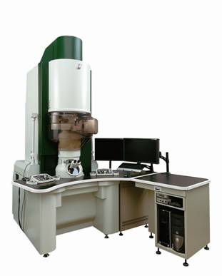
The year 2009 marks the introduction of a new generation of Transmission Electron Microscope (TEM) for JEOL, as well as the 60th anniversary of the company with the longest history of innovation and leadership in electron microscopy. JEOL is pleased to introduce the new JEM-ARM200F atomic resolution analytical microscope.
JEOL Unveils Highest Resolution 200kV Aberration-corrected Scanning/Transmission Electron Microscope (S/TEM)
Peabody, MA | Posted on March 10th, 2009According to JEOL USA, the company's U.S. subsidiary, JEOL has unveiled its new JEM-ARM200F atomic resolution analytical microscope, setting a new benchmark for advanced, aberration-corrected S/TEM technology with the highest resolution commercially available in its class. Through a rigorous development and design program inspired by JEOL customers, the JEOL team has produced an entirely new platform of TEM that achieves a guaranteed HAADF-STEM (high angle annular dark field) resolution of 80 picometers, or 0.08 nanometers.
Enhanced Analytical S/TEM
With advanced analytical capabilities, the JEM-ARM200F enables both atom-by-atom imaging resolution and unmatched spatial resolution for atom-to-atom chemical mapping of materials, including EDS (energy-dispersive x-ray spectroscopy) and EELS (electron energy-loss spectroscopy). The completely new electron column design integrates S/TEM with Cs correction for atomic spatial energy resolution combined with high probe currents for microanalysis.
Ultimate Stability at the Sub-Nanometer Scale
The JEM-ARM200F offers the ultimate stability for imaging and analysis at the sub-nanometer scale. The electron column is isolated from the environmental disturbances found in most labs. A superior shielding design safeguards the ultrahigh-powered optics from airflow, vibration, and acoustical interference. Additional shielding ensures protection from electronic interference, magnetic fields, and thermal fluctuations.
Integrated Software Automation
The latest in software automation has been designed into the new ARM200F, with tomography and holography simplified by a user-friendly GUI.
First U.S. Installation in World-renowned Researcher's Lab
The University of Texas at San Antonio (UTSA) will be the site of the first installation of the new JEM-ARM200F. The microscope will be housed in the Advanced Microscopy Laboratory under the supervision of world-renowned researcher Miguel Yacaman, chair of the College of Sciences' Department of Physics and Astronomy. There, it will support first-class research in nanotechnology, materials science, medicine, biology, chemistry and engineering.
Backed by Award-winning Service and Support
JEOL USA is renowned for its unrivaled applications expertise and training, plus its comprehensive, award-winning 24/7 service.
####
About JEOL USA
JEOL is a world leader in electron optical equipment and instrumentation for high-end scientific and industrial research and development. Core product groups include electron microscopes (SEMs and TEMs), instruments for the semiconductor industry (electron beam lithography and a series of defect review and inspection tools), and analytical instruments including mass spectrometers, NMRs and ESRs.
JEOL USA, Inc., is a wholly owned subsidiary of JEOL, Ltd., Japan, was incorporated in the United States in 1962. The company has 13 regional service centers that offer unlimited emergency service and support in the U.S.
For more information, please click here
Contacts:
JEOL USA, Inc.
11 Dearborn Road
Peabody, MA 01960
978-535-5900
Pamela Mansfield
Marketing Communications
JEOL USA
11 Dearborn Road
Peabody, MA 01966
Copyright © JEOL USA
If you have a comment, please Contact us.Issuers of news releases, not 7th Wave, Inc. or Nanotechnology Now, are solely responsible for the accuracy of the content.
| Related News Press |
News and information
![]() Quantum computer improves AI predictions April 17th, 2026
Quantum computer improves AI predictions April 17th, 2026
![]() Flexible sensor gains sensitivity under pressure April 17th, 2026
Flexible sensor gains sensitivity under pressure April 17th, 2026
![]() A reusable chip for particulate matter sensing April 17th, 2026
A reusable chip for particulate matter sensing April 17th, 2026
![]() Detecting vibrational quantum beating in the predissociation dynamics of SF6 using time-resolved photoelectron spectroscopy April 17th, 2026
Detecting vibrational quantum beating in the predissociation dynamics of SF6 using time-resolved photoelectron spectroscopy April 17th, 2026
Imaging
![]() Simple algorithm paired with standard imaging tool could predict failure in lithium metal batteries August 8th, 2025
Simple algorithm paired with standard imaging tool could predict failure in lithium metal batteries August 8th, 2025
Announcements
![]() A fundamentally new therapeutic approach to cystic fibrosis: Nanobody repairs cellular defect April 17th, 2026
A fundamentally new therapeutic approach to cystic fibrosis: Nanobody repairs cellular defect April 17th, 2026
![]() UC Irvine physicists discover method to reverse �quantum scrambling� : The work addresses the problem of information loss in quantum computing system April 17th, 2026
UC Irvine physicists discover method to reverse �quantum scrambling� : The work addresses the problem of information loss in quantum computing system April 17th, 2026
Tools
![]() Metasurfaces smooth light to boost magnetic sensing precision January 30th, 2026
Metasurfaces smooth light to boost magnetic sensing precision January 30th, 2026
![]() From sensors to smart systems: the rise of AI-driven photonic noses January 30th, 2026
From sensors to smart systems: the rise of AI-driven photonic noses January 30th, 2026
![]() Japan launches fully domestically produced quantum computer: Expo visitors to experience quantum computing firsthand August 8th, 2025
Japan launches fully domestically produced quantum computer: Expo visitors to experience quantum computing firsthand August 8th, 2025
|
|
||
|
|
||
| The latest news from around the world, FREE | ||
|
|
||
|
|
||
| Premium Products | ||
|
|
||
|
Only the news you want to read!
Learn More |
||
|
|
||
|
Full-service, expert consulting
Learn More |
||
|
|
||


