Home > Press > Lasers achieve world record tunability
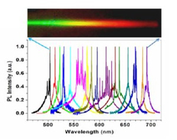 |
| Top: real color image of the nanowire wafer with color reflecting the bandgap tuning from left to right. Bottom: lasing spectra measured at 16 spots along the length of the wafer, showing spatial wavelength tunability of 200 nm. |
Abstract:
A single semiconductor laser chip with world-record wavelength tuning range of 200 nm—from 500 to 700 nm—has been demonstrated by a research team led by Cun-Zheng Ning, a professor in the Department of Electrical Engineering in the Ira A. Fulton School of Engineering at Arizona State Univ.
Lasers achieve world record tunability
Tempe, AZ | Posted on February 16th, 2009
Widely tunable semiconductor lasers offer a wide range of applications, ranging from spectroscopy, telecommunication, and on-chip biological and chemical detection. But achieving a widely tunable laser has been difficult due to limited lattice mismatch allowed in the standard epitaxial-based approach, since wavelength of light emission is determined by the bandgaps of semiconductors involved. Widely tunable lasers require alloy semiconductors with similarly tunable bandgaps, which are in turn determined by alloy composition, are usually limited by lattice mismatch with the chosen substrate.
With nanowire technology, the lattice mismatch limitation has been largely relaxed or removed completely. Thus it becomes possible in principle to grow alloy semiconductors of widely changing composition on a single substrate.
By carefully engineering and controlling the growth temperature and other parameters, the team was successful in growing ternary alloy CdSxSe1-x nanowires with composition x changing from 0 to 1 continuously from one end of the substrate to the other. As a result, the wafer has a continuous spatial grading of bandgaps between 1.75 eV and 2.5 eV, or in terms of the wavelength, between 500 and 700 nm.
Since the wafer is covered by nanowires that individually can act as nanolasers, numerous such nanolasers of continuously tuning wavelength are formed by a single growth on a single substrate. Under optical pumping, the team was able to show that each spot along the wafer length showing lasing behavior, as shown in the figure attached.
Such extremely wide tunable lasers are expected to have many potential applications. Tunable laser sources are vital elements for spectroscopic applications from research laboratories to molecular finger-print based field detection and sensing. They can act as multi-agent excitation light sources for florescence chip-based biological or chemical detections. They can also be used for multiplexing or de-multiplexing for chip-based communication applications. Many more applications can be explored, once such lasers are made electrically driven.
Ning's research group is currently working to extend the tunability to an even wider wavelength range and is developing several applications of such unique alloy materials in solar cells, detection, lighting and displays. In each of these applications, the unique materials capability is going to significantly improve the performance of the devices.
Team members include Dr. Ning's group at ASU, Dr. Anlian Pan, Weichang Zhou, Dr. Eunice Leong, Dr. Ruibin Liu, and Dr. Alan Chin, and his collaborator, Dr. B.S. Zou of Hunan University, China. For more information, contact Prof. Cun-Zheng Ning, (480) 965 7421; web: http://nanophotonics.asu.edu
The results are reported in a paper in a recent online version of the American Chemical Society journal Nano Letters. A log-in is required at pubs.acs.org.ezproxy1.lib.asu.edu/doi/full/10.1021/nl803456k
The research was supported by Science Foundation of Arizona and by US Army Research Office
####
For more information, please click here
Copyright © Arizona State University
If you have a comment, please Contact us.Issuers of news releases, not 7th Wave, Inc. or Nanotechnology Now, are solely responsible for the accuracy of the content.
Bookmark:


| Related News Press |
News and information
![]() Quantum computer improves AI predictions April 17th, 2026
Quantum computer improves AI predictions April 17th, 2026
![]() Flexible sensor gains sensitivity under pressure April 17th, 2026
Flexible sensor gains sensitivity under pressure April 17th, 2026
![]() A reusable chip for particulate matter sensing April 17th, 2026
A reusable chip for particulate matter sensing April 17th, 2026
![]() Detecting vibrational quantum beating in the predissociation dynamics of SF6 using time-resolved photoelectron spectroscopy April 17th, 2026
Detecting vibrational quantum beating in the predissociation dynamics of SF6 using time-resolved photoelectron spectroscopy April 17th, 2026
Discoveries
![]() Quantum computer improves AI predictions April 17th, 2026
Quantum computer improves AI predictions April 17th, 2026
![]() Flexible sensor gains sensitivity under pressure April 17th, 2026
Flexible sensor gains sensitivity under pressure April 17th, 2026
![]() A reusable chip for particulate matter sensing April 17th, 2026
A reusable chip for particulate matter sensing April 17th, 2026
![]() Detecting vibrational quantum beating in the predissociation dynamics of SF6 using time-resolved photoelectron spectroscopy April 17th, 2026
Detecting vibrational quantum beating in the predissociation dynamics of SF6 using time-resolved photoelectron spectroscopy April 17th, 2026
Announcements
![]() A fundamentally new therapeutic approach to cystic fibrosis: Nanobody repairs cellular defect April 17th, 2026
A fundamentally new therapeutic approach to cystic fibrosis: Nanobody repairs cellular defect April 17th, 2026
![]() UC Irvine physicists discover method to reverse ‘quantum scrambling’ : The work addresses the problem of information loss in quantum computing system April 17th, 2026
UC Irvine physicists discover method to reverse ‘quantum scrambling’ : The work addresses the problem of information loss in quantum computing system April 17th, 2026
Photonics/Optics/Lasers
![]() Metasurfaces smooth light to boost magnetic sensing precision January 30th, 2026
Metasurfaces smooth light to boost magnetic sensing precision January 30th, 2026
![]() From sensors to smart systems: the rise of AI-driven photonic noses January 30th, 2026
From sensors to smart systems: the rise of AI-driven photonic noses January 30th, 2026
|
|
||
|
|
||
| The latest news from around the world, FREE | ||
|
|
||
|
|
||
| Premium Products | ||
|
|
||
|
Only the news you want to read!
Learn More |
||
|
|
||
|
Full-service, expert consulting
Learn More |
||
|
|
||