Home > Press > IMEC builds reliable 11 megapixel micro-mirror array for high-end industrial applications
 |
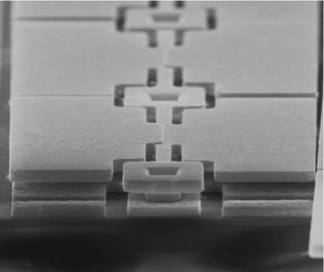
| Top view of individual mirrors and hinges |
Abstract:
At today's IEEE International Electron Devices Meeting, IMEC presents a monolithically integrated 11 megapixel micro-mirror array for high-end industrial applications, a world's first both in terms of pixel density and reliability. Each mirror in the array is 8μm x 8μm and can be individually tilted by the high-speed integrated CMOS circuitry underneath the array. This device fits in IMEC's CMORE initiative, which offers cost-effective solutions for continued system scaling, not by shrinking CMOS but by focusing on monolithic co-integration of heterogeneous technology.
IMEC builds reliable 11 megapixel micro-mirror array for high-end industrial applications
San Francisco, CA | Posted on December 16th, 2008IMEC's 10cm� 11 megapixel mirror array has a pixel density that is almost double that of comparable state-of-the-art micro-mirrors. And IMEC has demonstrated that its mirrors show no creep and meet a 1012 cycles mechanical lifetime. Integrated micro-mirror arrays such as this one, are used in, for example, video projection or lithography mask writers.
IMEC fabricated the 8�m mirrors on top of foundry high-voltage 0.18�m CMOS 200mm wafers with 6 interconnect levels. The array was built using IMEC's proprietary SiGe-based MEMS platform, meeting the mirror's mechanical reliability requirements, device flatness, and compatibility with high-speed CMOS. Poly-SiGe was chosen as structural material for the mirrors, instead of Al. Poly-SiGe solves many of the reliability issues of Al-based mirrors, and it is compatible with above CMOS processing, allowing a smooth integration with the CMOS chip below.
IMEC's CMORE initiative offers cost-effective solutions for monolithic co-integration of heterogeneous technologies. The services offered range from development-on-demand, over prototyping, to low-volume production. These services profit from the expertise in many research areas available at IMEC. The CMORE solutions are implemented in IMEC's 200mm fab with advanced packaging capabilities, such as 3D integration. The two process platforms involved are a 0.13�m CMOS process and a versatile SiGe above-IC MEMS process. On customer demand, the CMORE solution can be migrated to IMEC's 300mm fab.
####
About IMEC
IMEC is a world-leading independent research center in nanoelectronics and nanotechnology. IMEC vzw is headquartered in Leuven, Belgium, has a sister company in the Netherlands, IMEC-NL, offices in the US, China and Taiwan, and representatives in Japan. Its staff of more than 1650 people includes more than 500 industrial residents and guest researchers. In 2007, its revenue (P&L) was EUR 244.5 million.
IMEC�s More Moore research aims at semiconductor scaling towards sub-32nm nodes. With its More than Moore research, IMEC looks into technologies for nomadic embedded systems, wireless autonomous transducer solutions, biomedical electronics, photovoltaics, organic electronics and GaN power electronics.
IMEC�s research bridges the gap between fundamental research at universities and technology development in industry. Its unique balance of processing and system know-how, intellectual property portfolio, state-of-the-art infrastructure and its strong network worldwide position IMEC as a key partner for shaping technologies for future systems.
For more information, please click here
Contacts:
Jan Provoost
IMEC External Communications
T: +32 16 28 14 34
Copyright © IMEC
If you have a comment, please Contact us.Issuers of news releases, not 7th Wave, Inc. or Nanotechnology Now, are solely responsible for the accuracy of the content.
| Related News Press |
News and information
![]() Decoding hydrogen‑bond network of electrolyte for cryogenic durable aqueous zinc‑ion batteries January 30th, 2026
Decoding hydrogen‑bond network of electrolyte for cryogenic durable aqueous zinc‑ion batteries January 30th, 2026
![]() COF scaffold membrane with gate‑lane nanostructure for efficient Li+/Mg2+ separation January 30th, 2026
COF scaffold membrane with gate‑lane nanostructure for efficient Li+/Mg2+ separation January 30th, 2026
Chip Technology
![]() Metasurfaces smooth light to boost magnetic sensing precision January 30th, 2026
Metasurfaces smooth light to boost magnetic sensing precision January 30th, 2026
![]() Beyond silicon: Electronics at the scale of a single molecule January 30th, 2026
Beyond silicon: Electronics at the scale of a single molecule January 30th, 2026
![]() Lab to industry: InSe wafer-scale breakthrough for future electronics August 8th, 2025
Lab to industry: InSe wafer-scale breakthrough for future electronics August 8th, 2025
Announcements
![]() Decoding hydrogen‑bond network of electrolyte for cryogenic durable aqueous zinc‑ion batteries January 30th, 2026
Decoding hydrogen‑bond network of electrolyte for cryogenic durable aqueous zinc‑ion batteries January 30th, 2026
![]() COF scaffold membrane with gate‑lane nanostructure for efficient Li+/Mg2+ separation January 30th, 2026
COF scaffold membrane with gate‑lane nanostructure for efficient Li+/Mg2+ separation January 30th, 2026
Tools
![]() Metasurfaces smooth light to boost magnetic sensing precision January 30th, 2026
Metasurfaces smooth light to boost magnetic sensing precision January 30th, 2026
![]() From sensors to smart systems: the rise of AI-driven photonic noses January 30th, 2026
From sensors to smart systems: the rise of AI-driven photonic noses January 30th, 2026
![]() Japan launches fully domestically produced quantum computer: Expo visitors to experience quantum computing firsthand August 8th, 2025
Japan launches fully domestically produced quantum computer: Expo visitors to experience quantum computing firsthand August 8th, 2025
|
|
||
|
|
||
| The latest news from around the world, FREE | ||
|
|
||
|
|
||
| Premium Products | ||
|
|
||
|
Only the news you want to read!
Learn More |
||
|
|
||
|
Full-service, expert consulting
Learn More |
||
|
|
||


