Home > Press > SUSS MicroTec Boosts Nanotechnology with New Toolset for Mask Aligners
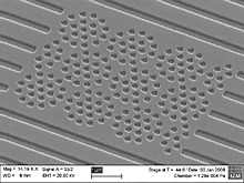 |
| 160nm wide holes positioned in concentric rings as used for photonics crystals. Printed in Amonil MM S4 on a SUSS MA6 Mask Aligner. Source: FhG/IZM |
Abstract:
SUSS MicroTec, supplier of innovative solutions for the 3D, MEMS, Advanced Packaging and Nanotechnology markets, has launched an advanced nanotechnology toolset for its Mask Aligners. The new Nano Imprint Lithography (NIL) tool enables SUSS Aligners to print resist thicknesses from less than 100 nanometers to a few hundred microns with a printing resolution down to a few nanometers.
SUSS MicroTec Boosts Nanotechnology with New Toolset for Mask Aligners
Garching, Germany | Posted on March 3rd, 2008UV-NIL is a low-cost production technology that is based on UV-curing. It has been developed as a cost-effective alternative to high-resolution e-beam lithography to print sub-20 nanometer geometries. UV-NIL applications with promising perspectives include semiconductor, MOEMS, NEMS and optoelectronic technologies.
This toolset can be upgraded on any previously installed SUSS MA6 Mask Aligner with very limited effort. Therefore SUSS MicroTec offers its customers an easy and quick step into the world of Nano.
"Nanotechnology represents a promising new business opportunity for SUSS MicroTec", said Rolf Wolf, General Manager of SUSS MicroTec Lithography division. "With the new UV-NIL tooling for mask aligners, SUSS MicroTec is once again providing market leadership for evolutionary as well as revolutionary innovative processing techniques."
####
About SUSS MicroTec
SUSS MicroTec machines are used by leading semiconductor manufacturers as well as renowned research institutes to make and test state-of-the art microchips and sensors. Many of the products you use in your daily life such as PDA's, GPS systems, cell phones etc. have at sometime been touched by equipment from SUSS MicroTec.
As a global supplier of production and test equipment for the semiconductor and related industries SUSS is especially present in markets including Advanced Packaging, MEMS, Nanotechnology, Compound Semiconductor, Silicon-On-Insulator and 3D Interconnect. Products include precision lithography tools (mask aligners, spin & spray coaters), wafer bonders and test systems.
For more information, please click here
Contacts:
Brigitte Wehrmann
Marketing Communications Manager Lithography Division
SUSS MicroTec Lithography GmbH
Schlei�heimer Str. 90
D 85748 Garching
Phone:+49 89 32007 237
Copyright © SUSS MicroTec
If you have a comment, please Contact us.Issuers of news releases, not 7th Wave, Inc. or Nanotechnology Now, are solely responsible for the accuracy of the content.
Bookmark:


| Related News Press |
News and information
![]() Quantum computer improves AI predictions April 17th, 2026
Quantum computer improves AI predictions April 17th, 2026
![]() Flexible sensor gains sensitivity under pressure April 17th, 2026
Flexible sensor gains sensitivity under pressure April 17th, 2026
![]() A reusable chip for particulate matter sensing April 17th, 2026
A reusable chip for particulate matter sensing April 17th, 2026
![]() Detecting vibrational quantum beating in the predissociation dynamics of SF6 using time-resolved photoelectron spectroscopy April 17th, 2026
Detecting vibrational quantum beating in the predissociation dynamics of SF6 using time-resolved photoelectron spectroscopy April 17th, 2026
Announcements
![]() A fundamentally new therapeutic approach to cystic fibrosis: Nanobody repairs cellular defect April 17th, 2026
A fundamentally new therapeutic approach to cystic fibrosis: Nanobody repairs cellular defect April 17th, 2026
![]() UC Irvine physicists discover method to reverse �quantum scrambling� : The work addresses the problem of information loss in quantum computing system April 17th, 2026
UC Irvine physicists discover method to reverse �quantum scrambling� : The work addresses the problem of information loss in quantum computing system April 17th, 2026
Tools
![]() Metasurfaces smooth light to boost magnetic sensing precision January 30th, 2026
Metasurfaces smooth light to boost magnetic sensing precision January 30th, 2026
![]() From sensors to smart systems: the rise of AI-driven photonic noses January 30th, 2026
From sensors to smart systems: the rise of AI-driven photonic noses January 30th, 2026
![]() Japan launches fully domestically produced quantum computer: Expo visitors to experience quantum computing firsthand August 8th, 2025
Japan launches fully domestically produced quantum computer: Expo visitors to experience quantum computing firsthand August 8th, 2025
Photonics/Optics/Lasers
![]() Metasurfaces smooth light to boost magnetic sensing precision January 30th, 2026
Metasurfaces smooth light to boost magnetic sensing precision January 30th, 2026
![]() From sensors to smart systems: the rise of AI-driven photonic noses January 30th, 2026
From sensors to smart systems: the rise of AI-driven photonic noses January 30th, 2026
|
|
||
|
|
||
| The latest news from around the world, FREE | ||
|
|
||
|
|
||
| Premium Products | ||
|
|
||
|
Only the news you want to read!
Learn More |
||
|
|
||
|
Full-service, expert consulting
Learn More |
||
|
|
||