Home > Press > No limits to silicon integrated circuits
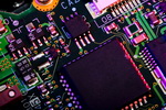 |
| New semiconductor microlasers with silicon wave guides will speed up data transfer � Shutterstock |
Abstract:
Microchip processing technology is being updated at faster and faster rates in our age of silicon chip wizardry. By the time you unpack your smart new laptop or digital camera the technology that went into making it is already becoming outdated. But a solution to the problem is now at hand. Researchers working on a project called PICMOS, with EU funding of EUR 2.5 million, have developed new technologies to produce and combine semiconductor microlasers with silicon wave guides for new, efficient and powerful optical connections.
No limits to silicon integrated circuits
Europe | Posted on February 13th, 2008Traditionally tiny copper wires connect different areas of integrated circuits, but these are limited in their use as they will soon start limiting microchip processing speeds. Since the birth of microchip technology, the miniaturisation of microchips has continued relentlessly with the number of transistors able to be fitted into an integrated circuit doubling on average every two years.
Microchips that are based on silicon wafers are now nearing their limits because the physical properties of near nanoscale silicon integrated circuits are beginning to interfere with their performance. The speed of data transfer in the integrated circuits is slowing down because the data is currently being sent as electrons through copper wires known as copper interconnects.
'Copper wire interconnects place serious limitations on the performance of silicon integrated circuits,' Dries Van Thourhout from Ghent University's Photonics Research Group and Belgium's IMEC, a micro- and nano-electronics research centre, told ICT Results.
'It is hard to transmit data down these interconnects in a sufficiently fast power-efficient way. It is a problem of bandwidth and copper will not be able to cope with the processing power of tomorrow's microchips.'
Using optical connects would be far more convenient than copper ones as opticals use light instead of electrons to relay data. They also have the capacity to be far more efficient at transmitting data, but using the same or less power. Instead of traveling along copper wires, they travel along wave guides that are made of silicon rather than glass.
'Lots of research has shown that you can etch wave guides for photons into silicon,' Van Thourhout is quoted as saying. 'This is great because you are using the same materials and fabrication technologies as you do to make integrated circuits. But there is one significant drawback: it is extremely hard to get light out of silicon.'
Part of the project research involved the development of indium-phosphate lasers etched with a diameter of just 7�m which is small enough to integrate several thousand onto a 2cm x 2cm silicon chip. These could be used in many ways, for example in miniature optical sensors such as strain detectors or they could be used to build inexpensive, but powerful optical biosensors.
At the moment the cost of producing the lasers is too high for mass production although the results of the research are encouraging. A follow-up project called WADIMOS which is also EU-funded is to carry on the PICMOS research.
####
For more information, please click here
Contacts:
DIRECTORATE-GENERAL FOR RESEARCH
European Commission
SDME 2/2
B-1049 Brussels - Belgium
http://ec.europa.eu/dgs/research/index_en.html
Copyright © European Commission
If you have a comment, please Contact us.Issuers of news releases, not 7th Wave, Inc. or Nanotechnology Now, are solely responsible for the accuracy of the content.
Bookmark:


| Related News Press |
News and information
![]() Quantum computer improves AI predictions April 17th, 2026
Quantum computer improves AI predictions April 17th, 2026
![]() Flexible sensor gains sensitivity under pressure April 17th, 2026
Flexible sensor gains sensitivity under pressure April 17th, 2026
![]() A reusable chip for particulate matter sensing April 17th, 2026
A reusable chip for particulate matter sensing April 17th, 2026
![]() Detecting vibrational quantum beating in the predissociation dynamics of SF6 using time-resolved photoelectron spectroscopy April 17th, 2026
Detecting vibrational quantum beating in the predissociation dynamics of SF6 using time-resolved photoelectron spectroscopy April 17th, 2026
Govt.-Legislation/Regulation/Funding/Policy
![]() Quantum computer improves AI predictions April 17th, 2026
Quantum computer improves AI predictions April 17th, 2026
![]() Metasurfaces smooth light to boost magnetic sensing precision January 30th, 2026
Metasurfaces smooth light to boost magnetic sensing precision January 30th, 2026
![]() New imaging approach transforms study of bacterial biofilms August 8th, 2025
New imaging approach transforms study of bacterial biofilms August 8th, 2025
Chip Technology
![]() A reusable chip for particulate matter sensing April 17th, 2026
A reusable chip for particulate matter sensing April 17th, 2026
![]() Metasurfaces smooth light to boost magnetic sensing precision January 30th, 2026
Metasurfaces smooth light to boost magnetic sensing precision January 30th, 2026
Optical computing/Photonic computing
![]() ICFO researchers overcome long-standing bottleneck in single photon detection with twisted 2D materials August 8th, 2025
ICFO researchers overcome long-standing bottleneck in single photon detection with twisted 2D materials August 8th, 2025
![]() Programmable electron-induced color router array May 14th, 2025
Programmable electron-induced color router array May 14th, 2025
Announcements
![]() A fundamentally new therapeutic approach to cystic fibrosis: Nanobody repairs cellular defect April 17th, 2026
A fundamentally new therapeutic approach to cystic fibrosis: Nanobody repairs cellular defect April 17th, 2026
![]() UC Irvine physicists discover method to reverse �quantum scrambling� : The work addresses the problem of information loss in quantum computing system April 17th, 2026
UC Irvine physicists discover method to reverse �quantum scrambling� : The work addresses the problem of information loss in quantum computing system April 17th, 2026
|
|
||
|
|
||
| The latest news from around the world, FREE | ||
|
|
||
|
|
||
| Premium Products | ||
|
|
||
|
Only the news you want to read!
Learn More |
||
|
|
||
|
Full-service, expert consulting
Learn More |
||
|
|
||