Home > Press > Sketching on silicon
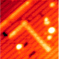 |
| Figure 1: Continuous molecular lines with perpendicular geometries can be drawn on silicon substrates using two different compounds that grow in different directions when they react with the surface atoms. Reproduced with permission from JACS 129, 12304�12309 (2007). Copyright (2007) the American Chemical Society |
Abstract:
Two different chemical compounds can be used to draw perpendicular molecular lines on the surface of silicon substrates
Sketching on silicon
Japan | Posted on February 1st, 2008Silicon is the workhorse material of the semiconductor industry because it is on this element that the integrated circuits of modern microprocessor devices are built. In order to satisfy the ever-increasing speed and power demands of computing, the miniaturization of such electronic components is the focus of much research.
So-called top-down methods used to carve ever-smaller features into the surface of silicon wafers will result in performance benefits for a little longer, but there are size limits to which these structures can be practically reduced. An alternative fabrication approach, however, relies upon the bottom-up assembly of molecular building blocks to form nanoscale electronic components.
Now, Maki Kawai and colleagues from RIKEN's Discovery Research Institute in Wako, have discovered a way to �draw' perpendicular lines�made from different molecules�on silicon surfaces that comprise pairs of atoms, known as dimers, aligned in parallel rows1. Writing in the Journal of the American Chemical Society, they found that acetone�a small organic compound�readily forms straight molecular lines along the rows of silicon dimers on these substrates.
The silicon substrate was first exposed to atomic hydrogen, resulting in the formation of silicon-hydrogen bonds. A small number of the silicon atoms do not react, however, and these so-called �dangling-bond sites' are quite reactive and can form bonds with organic molecules. When an acetone molecule becomes fixed to the surface by reacting with a dangling-bond site, a new dangling-bond site is created in the adjacent silicon dimer in the row, setting off a chain reaction in which more acetone molecules bond to the surface to form a molecular line.
Kawai and co-workers went on to show that acetone lines can be grown from the ends of lines formed from other molecules on the same silicon surface. In contrast with acetone, molecules of a compound called allylmercaptan form lines in a direction perpendicular to the rows of silicon dimmers (Fig. 1). In this way, mutually perpendicular lines can be formed on these silicon surfaces, since their direction can be simply controlled by changing the gas feed to the surface.
Because dangling-bond sites can also be produced at predefined positions on the surface with a scanning tunneling microscope, the origin of the lines can be precisely controlled. The ability to form molecular arrays with carefully controlled geometries on a material around which the semiconductor industry revolves could have significant implications for the rapidly developing field of molecular electronics.
Reference
1. Hossain, Md. Z., Kato, H. S. & Kawai, M. Selective chain reaction of acetone leading to the successive growth of mutually perpendicular molecular lines on the Si(100)-(2x1)-H surface. Journal of the American Chemical Society 129, 12304-12309 (2007).
####
About Riken
RIKEN is one of Japan�s largest research organisations with institutes and centres in various locations in Japan (see www.riken.jp/engn/r-world/link/index.html). RIKEN�s 3000+ researchers publish several hundred research articles in top scientific and technical journals every year across a broad spectrum of disciplines in physics, chemistry, biology, medicine, earth science and in many areas of technology, and the number of articles is growing year on year.
For more information, please click here
Copyright © Riken
If you have a comment, please Contact us.Issuers of news releases, not 7th Wave, Inc. or Nanotechnology Now, are solely responsible for the accuracy of the content.
Bookmark:


| Related News Press |
News and information
![]() Quantum computer improves AI predictions April 17th, 2026
Quantum computer improves AI predictions April 17th, 2026
![]() Flexible sensor gains sensitivity under pressure April 17th, 2026
Flexible sensor gains sensitivity under pressure April 17th, 2026
![]() A reusable chip for particulate matter sensing April 17th, 2026
A reusable chip for particulate matter sensing April 17th, 2026
![]() Detecting vibrational quantum beating in the predissociation dynamics of SF6 using time-resolved photoelectron spectroscopy April 17th, 2026
Detecting vibrational quantum beating in the predissociation dynamics of SF6 using time-resolved photoelectron spectroscopy April 17th, 2026
Chip Technology
![]() A reusable chip for particulate matter sensing April 17th, 2026
A reusable chip for particulate matter sensing April 17th, 2026
![]() Metasurfaces smooth light to boost magnetic sensing precision January 30th, 2026
Metasurfaces smooth light to boost magnetic sensing precision January 30th, 2026
Discoveries
![]() Quantum computer improves AI predictions April 17th, 2026
Quantum computer improves AI predictions April 17th, 2026
![]() Flexible sensor gains sensitivity under pressure April 17th, 2026
Flexible sensor gains sensitivity under pressure April 17th, 2026
![]() A reusable chip for particulate matter sensing April 17th, 2026
A reusable chip for particulate matter sensing April 17th, 2026
![]() Detecting vibrational quantum beating in the predissociation dynamics of SF6 using time-resolved photoelectron spectroscopy April 17th, 2026
Detecting vibrational quantum beating in the predissociation dynamics of SF6 using time-resolved photoelectron spectroscopy April 17th, 2026
Announcements
![]() A fundamentally new therapeutic approach to cystic fibrosis: Nanobody repairs cellular defect April 17th, 2026
A fundamentally new therapeutic approach to cystic fibrosis: Nanobody repairs cellular defect April 17th, 2026
![]() UC Irvine physicists discover method to reverse �quantum scrambling� : The work addresses the problem of information loss in quantum computing system April 17th, 2026
UC Irvine physicists discover method to reverse �quantum scrambling� : The work addresses the problem of information loss in quantum computing system April 17th, 2026
|
|
||
|
|
||
| The latest news from around the world, FREE | ||
|
|
||
|
|
||
| Premium Products | ||
|
|
||
|
Only the news you want to read!
Learn More |
||
|
|
||
|
Full-service, expert consulting
Learn More |
||
|
|
||