Home > Press > Measurements from the Edge: Magnetic Properties of Thin Films
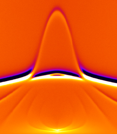 |
| Spectroscopic image showing the microwave-frequency magnetic resonances of an array of parallel, metallic thin film nanowires ("stripes"). The peak in the center is due to resonances occurring at the stripe edges while the strong horizontal bar is due to resonances in the body of the stripes.
Credit: Brian Maranville, NIST |
Abstract:
Materials researchers at the National Institute of Standards and Technology (NIST), together with colleagues from IBM and the Massachusetts Institute of Technology, have pushed the measurement of thin films to the edge—literally—to produce the first data on how the edges of metallic thin films contribute to their magnetic properties. Their results may impact the design of future nanoscale electronics.
Measurements from the Edge: Magnetic Properties of Thin Films
GAITHERSBURG, MD | Posted on September 28th, 2007Ferromagnetic thin films of metallic materials—ranging in thickness from fractions of a nanometer to several micrometers—are layered in patterns on a substrate (such as silicon) during the manufacture of many microelectronic devices that use magnetic properties, such as computer hard drives.
While methods for measuring the magnetic properties of ferromagnetic thin films have existed for some time, there currently is no way to define those properties for the edges of the film. On a relatively large-scale device, this doesn't matter much. However, as microelectronic components get smaller and smaller, the edge becomes a bigger and bigger fraction of the surface, eventually becoming the thin film's dominant surface and the driver of its magnetic character. (Shrink a disk by half and the top surface area is reduced by a factor of four while the length of the edge is only halved.)
A research team from NIST, IBM and MIT recently demonstrated a spectroscopic technique for measuring the magnetic properties of the edges of nickel-iron alloy thin films patterned in an array of parallel nanowires (called "stripes") atop a silicon disk. The researchers beamed microwaves of different frequencies over the stripes and measured the magnetic resonances that resulted. Because a thin film's edge resonates differently from its center, the researchers were able to determine which data—and subsequently, which magnetic behaviors—were attributable to the edge.
In its first trials, the new technique has been used to measure how the magnetic properties of the thin film edge are affected by the thickness of the film and the processing conditions during the stripe patterning. Data gained from the study of stripes with widths of 250 to 1,000 nanometers will be used to predict the behavior of similar structures at the nanoscale level (100 nanometers or less).
####
About NIST
From automated teller machines and atomic clocks to mammograms and semiconductors, innumerable products and services rely in some way on technology, measurement, and standards provided by the National Institute of Standards and Technology.
Founded in 1901, NIST is a non-regulatory federal agency within the U.S. Department of Commerce. NIST's mission is to promote U.S. innovation and industrial competitiveness by advancing measurement science, standards, and technology in ways that enhance economic security and improve our quality of life.
For more information, please click here
Contacts:
Michael E. Newman
(301) 975-3025
Copyright © NIST
If you have a comment, please Contact us.Issuers of news releases, not 7th Wave, Inc. or Nanotechnology Now, are solely responsible for the accuracy of the content.
Bookmark:


| Related News Press |
Memory Technology
![]() Researchers tackle the memory bottleneck stalling quantum computing October 3rd, 2025
Researchers tackle the memory bottleneck stalling quantum computing October 3rd, 2025
![]() First real-time observation of two-dimensional melting process: Researchers at Mainz University unveil new insights into magnetic vortex structures August 8th, 2025
First real-time observation of two-dimensional melting process: Researchers at Mainz University unveil new insights into magnetic vortex structures August 8th, 2025
![]() Utilizing palladium for addressing contact issues of buried oxide thin film transistors April 5th, 2024
Utilizing palladium for addressing contact issues of buried oxide thin film transistors April 5th, 2024
Nanoelectronics
![]() Lab to industry: InSe wafer-scale breakthrough for future electronics August 8th, 2025
Lab to industry: InSe wafer-scale breakthrough for future electronics August 8th, 2025
![]() Interdisciplinary: Rice team tackles the future of semiconductors Multiferroics could be the key to ultralow-energy computing October 6th, 2023
Interdisciplinary: Rice team tackles the future of semiconductors Multiferroics could be the key to ultralow-energy computing October 6th, 2023
![]() Key element for a scalable quantum computer: Physicists from Forschungszentrum Jülich and RWTH Aachen University demonstrate electron transport on a quantum chip September 23rd, 2022
Key element for a scalable quantum computer: Physicists from Forschungszentrum Jülich and RWTH Aachen University demonstrate electron transport on a quantum chip September 23rd, 2022
![]() Reduced power consumption in semiconductor devices September 23rd, 2022
Reduced power consumption in semiconductor devices September 23rd, 2022
Discoveries
![]() Quantum computer improves AI predictions April 17th, 2026
Quantum computer improves AI predictions April 17th, 2026
![]() Flexible sensor gains sensitivity under pressure April 17th, 2026
Flexible sensor gains sensitivity under pressure April 17th, 2026
![]() A reusable chip for particulate matter sensing April 17th, 2026
A reusable chip for particulate matter sensing April 17th, 2026
![]() Detecting vibrational quantum beating in the predissociation dynamics of SF6 using time-resolved photoelectron spectroscopy April 17th, 2026
Detecting vibrational quantum beating in the predissociation dynamics of SF6 using time-resolved photoelectron spectroscopy April 17th, 2026
Materials/Metamaterials/Magnetoresistance
![]() First real-time observation of two-dimensional melting process: Researchers at Mainz University unveil new insights into magnetic vortex structures August 8th, 2025
First real-time observation of two-dimensional melting process: Researchers at Mainz University unveil new insights into magnetic vortex structures August 8th, 2025
![]() Researchers unveil a groundbreaking clay-based solution to capture carbon dioxide and combat climate change June 6th, 2025
Researchers unveil a groundbreaking clay-based solution to capture carbon dioxide and combat climate change June 6th, 2025
![]() A 1960s idea inspires NBI researchers to study hitherto inaccessible quantum states June 6th, 2025
A 1960s idea inspires NBI researchers to study hitherto inaccessible quantum states June 6th, 2025
![]() Institute for Nanoscience hosts annual proposal planning meeting May 16th, 2025
Institute for Nanoscience hosts annual proposal planning meeting May 16th, 2025
Announcements
![]() A fundamentally new therapeutic approach to cystic fibrosis: Nanobody repairs cellular defect April 17th, 2026
A fundamentally new therapeutic approach to cystic fibrosis: Nanobody repairs cellular defect April 17th, 2026
![]() UC Irvine physicists discover method to reverse ‘quantum scrambling’ : The work addresses the problem of information loss in quantum computing system April 17th, 2026
UC Irvine physicists discover method to reverse ‘quantum scrambling’ : The work addresses the problem of information loss in quantum computing system April 17th, 2026
|
|
||
|
|
||
| The latest news from around the world, FREE | ||
|
|
||
|
|
||
| Premium Products | ||
|
|
||
|
Only the news you want to read!
Learn More |
||
|
|
||
|
Full-service, expert consulting
Learn More |
||
|
|
||