Home > Press > Drawing Nanoscale Features the Fast and Easy Way
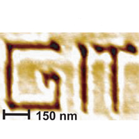 |
| The initials for the Georgia Institute of Technology written with the thermochemical nanolithography technique. (Image: Georgia Tech) |
Abstract:
Scientists at the Georgia Institute of Technology have developed a new technique for nanolithography that is extremely fast and capable of being used in a range of environments including air (outside a vacuum) and liquids. Researchers have demonstrated the technique, known as thermochemical nanolithography, as a proof of concept. The technique may allow industry to produce a variety of nanopatterned structures, including nanocircuits, at a speed and scale that could make their manufacture commercially viable. The research, which has potential applications for fields ranging from the electronics industry to nanofluidics to medicine, appeared earlier this year in the journal Nano Letters.
Drawing Nanoscale Features the Fast and Easy Way
Atlanta, GA | Posted on September 10th, 2007The technique is surprisingly simple. Using an atomic force microscope (AFM), researchers heat a silicon tip and run it over a thin polymer film. The heat from the tip induces a chemical reaction at the surface of the film. This reaction changes the film's chemical reactivity and transforms it from a hydrophobic substance to a hydrophilic one that can stick to other molecules. The technique is extremely fast and can write at speeds faster than millimeters per second. That's orders of magnitude faster than the widely used dip-pen nanolithography (DPN), which routinely clocks at a speed of 0.0001 millimeters per second.
Using the new technique, researchers were able to pattern with dimensions down to 12 nanometers in width in a variety of environments. Other techniques typically require the addition of other chemicals to be transferred to the surface or the presence of strong electric fields. TCNL doesn't have these requirements and can be used in humid environments outside a vacuum. By using an array of AFM tips developed by IBM, TCNL also has the potential to be massively scalable, allowing users to independently draw features with thousands of tips at a time rather than just one.
"Thermochemical nanolithography is a rapid and versatile technique that puts us much closer to achieving the speeds required for commercial applications," said Elisa Riedo, assistant professor in Georgia Tech's School of Physics. "Because we're not transferring any materials from the AFM tip to the polymer surface (we are only heating it to change its chemical structure) this method can be intrinsically faster than other techniques."
It's the heated AFM tips that are one key to the new technique. Designed and fabricated by a group led by William King at the University of Illinois, the tips can reach temperatures hotter than 1,000 degrees Celsius. They can also be repeatedly heated and cooled 1 million times per second.
"The heated tip is the world's smallest controllable heat source," said King.
TCNL is also tunable. By varying the amount of heat, the speed and the distance of the tip to the polymer, researchers can introduce topographical changes or modulate the range of chemical changes produced in the material.
"By changing the chemistry of the polymer, we've shown that we can selectively attach new substances, like metal ions or dyes to the patterned regions of the film in order to greatly increase the technique's functionality," said Seth Marder, professor in Tech's School of Chemistry and Biochemistry and director of the Center for Organic Photonics and Electronics. Marder's group developed the thermally switchable polymers used in this study.
"We expect thermochemical nanolithography to be widely adopted because it's conceptually simple and can be broadly applied," said Marder. "The scope is limited only by one's imagination to develop new chemistries and applications."
For nanolithography to be commercially viable, it must be able to write at high speeds, be used in a variety of environments and write on a variety of materials. While the technique demonstrated here doesn't yet allow writing at the centimeters per second rate that would be ideal, it does put researchers much closer to the goal than previous techniques. Once perfected, nanolithography could be used to draw nanocircuits for the electronics industry, create nanochannels for nanofluidics devices or be adapted for drug delivery or biosensing technologies.
The research was supported by the National Science Foundation's Center for Materials and Devices for Information Technology Research, the U.S. Department of Energy, the National Science Foundation, the Georgia Institute of Technology Research Foundation, the GT College of Sciences Cutting Edge Research Award and ONR Nanoelectronics. In addition to Riedo, Marder and King, the interdisciplinary research team consisted of Robert Szoszkiewicz, Takashi Okada, Simon Jones and Tai-De Li from Georgia Tech.
####
About Georgia Institute of Technology
The Georgia Institute of Technology is one of the nation's premiere research universities. Ranked seventh among U.S. News & World Report's top public universities, Georgia Tech's more than 18,000 students are enrolled in its Colleges of Architecture, Computing, Engineering, Liberal Arts, Management and Sciences. Tech is among the nation's top producers of women and African-American engineers. The Institute offers research opportunities to both undergraduate and graduate students and is home to more than 100 interdisciplinary units plus the Georgia Tech Research Institute.
For more information, please click here
Contacts:
David Terraso
Institute Communications & Public Affairs
404-385-2966
Copyright © Georgia Institute of Technology
If you have a comment, please Contact us.Issuers of news releases, not 7th Wave, Inc. or Nanotechnology Now, are solely responsible for the accuracy of the content.
Bookmark:


| Related News Press |
Chip Technology
![]() A reusable chip for particulate matter sensing April 17th, 2026
A reusable chip for particulate matter sensing April 17th, 2026
![]() Metasurfaces smooth light to boost magnetic sensing precision January 30th, 2026
Metasurfaces smooth light to boost magnetic sensing precision January 30th, 2026
Nanoelectronics
![]() Lab to industry: InSe wafer-scale breakthrough for future electronics August 8th, 2025
Lab to industry: InSe wafer-scale breakthrough for future electronics August 8th, 2025
![]() Interdisciplinary: Rice team tackles the future of semiconductors Multiferroics could be the key to ultralow-energy computing October 6th, 2023
Interdisciplinary: Rice team tackles the future of semiconductors Multiferroics could be the key to ultralow-energy computing October 6th, 2023
![]() Key element for a scalable quantum computer: Physicists from Forschungszentrum J�lich and RWTH Aachen University demonstrate electron transport on a quantum chip September 23rd, 2022
Key element for a scalable quantum computer: Physicists from Forschungszentrum J�lich and RWTH Aachen University demonstrate electron transport on a quantum chip September 23rd, 2022
![]() Reduced power consumption in semiconductor devices September 23rd, 2022
Reduced power consumption in semiconductor devices September 23rd, 2022
Discoveries
![]() Quantum computer improves AI predictions April 17th, 2026
Quantum computer improves AI predictions April 17th, 2026
![]() Flexible sensor gains sensitivity under pressure April 17th, 2026
Flexible sensor gains sensitivity under pressure April 17th, 2026
![]() A reusable chip for particulate matter sensing April 17th, 2026
A reusable chip for particulate matter sensing April 17th, 2026
![]() Detecting vibrational quantum beating in the predissociation dynamics of SF6 using time-resolved photoelectron spectroscopy April 17th, 2026
Detecting vibrational quantum beating in the predissociation dynamics of SF6 using time-resolved photoelectron spectroscopy April 17th, 2026
Announcements
![]() A fundamentally new therapeutic approach to cystic fibrosis: Nanobody repairs cellular defect April 17th, 2026
A fundamentally new therapeutic approach to cystic fibrosis: Nanobody repairs cellular defect April 17th, 2026
![]() UC Irvine physicists discover method to reverse �quantum scrambling� : The work addresses the problem of information loss in quantum computing system April 17th, 2026
UC Irvine physicists discover method to reverse �quantum scrambling� : The work addresses the problem of information loss in quantum computing system April 17th, 2026
Tools
![]() Metasurfaces smooth light to boost magnetic sensing precision January 30th, 2026
Metasurfaces smooth light to boost magnetic sensing precision January 30th, 2026
![]() From sensors to smart systems: the rise of AI-driven photonic noses January 30th, 2026
From sensors to smart systems: the rise of AI-driven photonic noses January 30th, 2026
![]() Japan launches fully domestically produced quantum computer: Expo visitors to experience quantum computing firsthand August 8th, 2025
Japan launches fully domestically produced quantum computer: Expo visitors to experience quantum computing firsthand August 8th, 2025
Printing/Lithography/Inkjet/Inks/Bio-printing/Dyes
![]() Presenting: Ultrasound-based printing of 3D materials�potentially inside the body December 8th, 2023
Presenting: Ultrasound-based printing of 3D materials�potentially inside the body December 8th, 2023
![]() Simple ballpoint pen can write custom LEDs August 11th, 2023
Simple ballpoint pen can write custom LEDs August 11th, 2023
![]() Disposable electronics on a simple sheet of paper October 7th, 2022
Disposable electronics on a simple sheet of paper October 7th, 2022
|
|
||
|
|
||
| The latest news from around the world, FREE | ||
|
|
||
|
|
||
| Premium Products | ||
|
|
||
|
Only the news you want to read!
Learn More |
||
|
|
||
|
Full-service, expert consulting
Learn More |
||
|
|
||