Home > News > Device allows naked eye to see motion of 10 nanometers
September 30th, 2004
Device allows naked eye to see motion of 10 nanometers
Abstract:
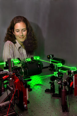
A new class of very small handheld devices can detect motion a thousand times more subtly than any tool known. "There was nothing in the [optics] literature to predict that this would happen," says Sandia National Laboratories researcher Dustin Carr of his group�s device, which reflects a bright light from a very small moving object.
Story:
Sandia creates motion detector 1,000 times more sensitive than any known
Device allows naked eye to see motion of 10 nanometers
Albuquerque, N.M. September 29, 2004
A new class of very small handheld devices can detect motion a thousand times more subtly than any tool known.
�There was nothing in the [optics] literature to predict that this would happen,� says Sandia National Laboratories researcher Dustin Carr of his group�s device, which reflects a bright light from a very small moving object.
Sandia is a National Nuclear Security Administration laboratory.
Carr, who earlier gained fame as a graduate student at Cornell for his creation of a nanoguitar, was selected this week by MIT�s science magazine Technology Review as one of the year�s top 100 researchers under the age of 35.
The patent-applied-for device will be the subject of an invited talk at the SPIE Optics East convention in Philadelphia in October, delivered by Sandia team member Bianca Keeler.
Like shadow pictures projected onto a wall by shining light through the fingers of one hand moving over the fingers of the other, the relatively simple measuring device depends upon a formerly unrecognized property of optics: light diffracted from very small gratings that move very small lateral distances undergoes a relatively big, and thus easily measurable, change in reflection. A motion of 10 nanometers can be seen by the naked eye, says Carr.
A nanometer is one-thousandth of a micron, which is one millionth of a meter.
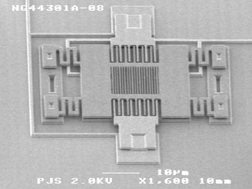
As for the device, size matters and small is crucial. �In standard MEMS [microelectromechanical] applications, though the devices are small, very few things that sell are dominated by a search for further miniaturization. There�s not a motivation in MEMS to make things still smaller as a matter of cost. Economics of scale for integrated circuits just don�t apply to MEMS. But our device couldn�t exist unless you made it this small,� he says. Features are in the 100-200 nanometer range, with 300 nm between top and bottom combs and 600 to 900 nm between comb teeth.
Sub-wavelength interference effects cause the visual display.
�Making use of the effect is fairly obvious once you realize it happens,� he says.
Fabricated out of polysilicon by standard lithography techniques like those used to make MEMS devices, the Sandia system uses two tiny comb-like structures (instead of fingers) laid one over each other. The bottom comb is locked rigidly in place. The top comb is secured only by horizontal springs. Any tiny motion sends the top comb skittering over the bottom comb, laterally deforming the grating. A very tiny disturbance changes by an unexpectedly large amount the amplitude of light � in the visible to near-infrared range � diffracted from a tiny laser beam shining upon the apparatus.
The measuring device, still in the laboratory stage, is in effect a kind of accelerometer, about the size of the inexpensive microelectromechanical devices that open automobile air bags. Fabricated by the same processes that mass-produce silicon computer chips, the device has multiple possible uses.
�If you can make very sensitive detectors very cheaply and very small, there are huge applications,� says Carr. �Made small, synchronized, cheap, and placed on every block, we could take data from all these sensors at once and measure the motion of the earth when there�s not an earthquake. So we could learn what leads up to one.�
Another use would be for skid and traction control in cars, detecting if the back end of the car is moving in a different direction from the front end.
�Such devices also could take the place of inertial navigation systems,� Carr says. These typically require large gyroscopes to keep commercial airplanes moving on a preset course. �We could have handheld-sized devices on Volkswagens that would work even in a tunnel.�
Other defense applications are possible, he says.
He sees a time frame of three to five years before the devices are available for use.
Says James Walker, former Director of Advanced Technologies at Tellium, Inc., former manager of the MEMS Network Element Sub-systems Group at Lucent, Bell Laboratories, and now an independent consultant and patent agent, �To my understanding, it is the first time anyone has tried to manipulate the optical near-field region in order to affect changes to the far-field characteristics of a grating. The ability to do this is a direct result of the nano-scale nature of the device. Due to its high responsivity-to-displacement ratio, I see it having significant, far-reaching application in areas as diverse as chemical sensing, infrared imaging, accelerometry, and displays.�
Sandia is a multiprogram laboratory operated by Sandia Corporation, a Lockheed Martin company, for the U.S. Department of Energy�s National Nuclear Security Administration. Sandia has major R&D responsibilities in national security, energy and environmental technologies, and economic competitiveness.
Media Contact:Neal Singer
nsinger@sandia.gov
(505) 845-7078
Copyright © SNL
If you have a comment, please us.
| Related News Press |
Possible Futures
![]() Decoding hydrogen‑bond network of electrolyte for cryogenic durable aqueous zinc‑ion batteries January 30th, 2026
Decoding hydrogen‑bond network of electrolyte for cryogenic durable aqueous zinc‑ion batteries January 30th, 2026
![]() COF scaffold membrane with gate‑lane nanostructure for efficient Li+/Mg2+ separation January 30th, 2026
COF scaffold membrane with gate‑lane nanostructure for efficient Li+/Mg2+ separation January 30th, 2026
Sensors
![]() Tiny nanosheets, big leap: A new sensor detects ethanol at ultra-low levels January 30th, 2026
Tiny nanosheets, big leap: A new sensor detects ethanol at ultra-low levels January 30th, 2026
![]() From sensors to smart systems: the rise of AI-driven photonic noses January 30th, 2026
From sensors to smart systems: the rise of AI-driven photonic noses January 30th, 2026
![]() Sensors innovations for smart lithium-based batteries: advancements, opportunities, and potential challenges August 8th, 2025
Sensors innovations for smart lithium-based batteries: advancements, opportunities, and potential challenges August 8th, 2025
Discoveries
![]() From sensors to smart systems: the rise of AI-driven photonic noses January 30th, 2026
From sensors to smart systems: the rise of AI-driven photonic noses January 30th, 2026
![]() Decoding hydrogen‑bond network of electrolyte for cryogenic durable aqueous zinc‑ion batteries January 30th, 2026
Decoding hydrogen‑bond network of electrolyte for cryogenic durable aqueous zinc‑ion batteries January 30th, 2026
![]() COF scaffold membrane with gate‑lane nanostructure for efficient Li+/Mg2+ separation January 30th, 2026
COF scaffold membrane with gate‑lane nanostructure for efficient Li+/Mg2+ separation January 30th, 2026
|
|
||
|
|
||
| The latest news from around the world, FREE | ||
|
|
||
|
|
||
| Premium Products | ||
|
|
||
|
Only the news you want to read!
Learn More |
||
|
|
||
|
Full-service, expert consulting
Learn More |
||
|
|
||


