Home > Press > EU Team Demonstrates Full Data-Transfer Silicon Photonics Module Delivering 100 Gb/s and Develops Building Blocks for Tb/s: COSMICC Project Breakthroughs ‘Will Answer Tremendous Market Needs with a Target Cost per Bit that Traditional Wavelength-Division Multiplexing Transceivers
 |
Abstract:
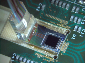
CEA-Leti today announced the demonstration of a fully packaged CWDM optical transceiver module with data transfer of 100 Gb/s per fiber with a low-power-consumption electronic chip co-integrated on the photonic chip. This silicon-photonics-based transceiver multiplexes two wavelengths at 50 Gb/s and is designed to meet the ever-increasing data-communication demands and energy use of data centers and supercomputers.
EU Team Demonstrates Full Data-Transfer Silicon Photonics Module Delivering 100 Gb/s and Develops Building Blocks for Tb/s: COSMICC Project Breakthroughs ‘Will Answer Tremendous Market Needs with a Target Cost per Bit that Traditional Wavelength-Division Multiplexing Transceivers
Grenoble, France | Posted on June 23rd, 2020The EU H2020 project, COSMICC, further developed all the required building blocks for a transmission rate of 200 Gb/s and beyond without temperature control with four 50-Gb/s wavelengths and by aggregating a large number of fibers. The key breakthroughs are the development of broadband and temperature-insensitive silicon nitride (SiN) multiplexing components on silicon (Si), the integration of hybrid III-V/Si lasers on the Si/SiN chips and a new high-count adiabatic fiber-coupling technique via SiN and polymer waveguides.
This demonstration opens the way to technology that allows a reduction in the cost, the power consumption and the packaging complexity and opens the way to reaching a very high aggregated data rate beyond terabits per second (Tb/s).
Starting with STMicroelectronics’ silicon photonics integration platform, the COSMICC project developed a coarse wavelength division multiplexing (CWDM) silicon-photonics transceiver in a packaged module at 100 Gb/s per fiber. It is scalable to 400 Gb/s and includes 3D assembly of a silicon photonic chip and its electronic control chip. The silicon photonic chip integrated high-performance 50 Gb/s NRZ optical modulators and photodetectors, and a two-channel CWDM multiplexer and demultiplexer. The control electronics was optimized to minimize energy consumption down to 5.7 pJ/bit per channel at 50 Gb/s data rate.
Separately, a library of enabling building blocks for higher data-rate datacenter interconnects was built on a SiN-enhanced silicon photonics platform, including new broadband and athermal SiN components and hybrid III-V/Si lasers. SiN, which is 10 times less sensitive to temperature than silicon, will dramatically reduce the transceiver cost and power consumption by eliminating the need for temperature control and will thus contribute to the reduction of the heat output and cooling costs of mega datacenters.
CEA-Leti scientist Ségolčne Olivier, who coordinated the EU project, said development of modulators and photodetectors at 50 Gb/s and their co-integration with their control electronics was a breakthrough that led to the low-power consumption 100 Gb/s transceiver module.
“In addition, the new building blocks are essential for addressing the need for terabit-per-second transceivers at low cost and low energy consumption to sustain the exponential growth of data traffic in datacenters and in high performance computing systems,” she explained.
“COSMICC’s technology will answer tremendous market needs with a target cost per bit that traditional WDM transceivers cannot meet,” Olivier said.
In addition to CEA-Leti, COSMICC consortium members include:
Industry: STMicroelectronics Italy & France, Vario-Optics, Seagate, Finisar
Academic & institutional: Université Paris Sud, Universita di Pavia, University of Southampton Optical Research Center, University of Saint Andrews, Cork Institute of Technology
Consultants: Ayming
####
About CEA Leti
Leti, a technology research institute at CEA, is a global leader in miniaturization technologies enabling smart, energy-efficient and secure solutions for industry. Founded in 1967, CEA-Leti pioneers micro-& nanotechnologies, tailoring differentiating applicative solutions for global companies, SMEs and startups. CEA-Leti tackles critical challenges in healthcare, energy and digital migration. From sensors to data processing and computing solutions, CEA-Leti’s multidisciplinary teams deliver solid expertise, leveraging world-class pre-industrialization facilities. With a staff of more than 1,900, a portfolio of 3,100 patents, 10,000 sq. meters of cleanroom space and a clear IP policy, the institute is based in Grenoble, France, and has offices in Silicon Valley and Tokyo. CEA-Leti has launched 65 startups and is a member of the Carnot Institutes network. Follow us on www.leti-cea.com and @CEA_Leti.
For more information, please click here
Contacts:
Press Contact
Agency
+33 6 74 93 23 47
Copyright © CEA Leti
If you have a comment, please Contact us.Issuers of news releases, not 7th Wave, Inc. or Nanotechnology Now, are solely responsible for the accuracy of the content.
Bookmark:


| Related News Press |
News and information
![]() Quantum computer improves AI predictions April 17th, 2026
Quantum computer improves AI predictions April 17th, 2026
![]() Flexible sensor gains sensitivity under pressure April 17th, 2026
Flexible sensor gains sensitivity under pressure April 17th, 2026
![]() A reusable chip for particulate matter sensing April 17th, 2026
A reusable chip for particulate matter sensing April 17th, 2026
![]() Detecting vibrational quantum beating in the predissociation dynamics of SF6 using time-resolved photoelectron spectroscopy April 17th, 2026
Detecting vibrational quantum beating in the predissociation dynamics of SF6 using time-resolved photoelectron spectroscopy April 17th, 2026
Possible Futures
![]() A fundamentally new therapeutic approach to cystic fibrosis: Nanobody repairs cellular defect April 17th, 2026
A fundamentally new therapeutic approach to cystic fibrosis: Nanobody repairs cellular defect April 17th, 2026
![]() UC Irvine physicists discover method to reverse ‘quantum scrambling’ : The work addresses the problem of information loss in quantum computing system April 17th, 2026
UC Irvine physicists discover method to reverse ‘quantum scrambling’ : The work addresses the problem of information loss in quantum computing system April 17th, 2026
Chip Technology
![]() A reusable chip for particulate matter sensing April 17th, 2026
A reusable chip for particulate matter sensing April 17th, 2026
![]() Metasurfaces smooth light to boost magnetic sensing precision January 30th, 2026
Metasurfaces smooth light to boost magnetic sensing precision January 30th, 2026
Memory Technology
![]() Researchers tackle the memory bottleneck stalling quantum computing October 3rd, 2025
Researchers tackle the memory bottleneck stalling quantum computing October 3rd, 2025
![]() First real-time observation of two-dimensional melting process: Researchers at Mainz University unveil new insights into magnetic vortex structures August 8th, 2025
First real-time observation of two-dimensional melting process: Researchers at Mainz University unveil new insights into magnetic vortex structures August 8th, 2025
![]() Utilizing palladium for addressing contact issues of buried oxide thin film transistors April 5th, 2024
Utilizing palladium for addressing contact issues of buried oxide thin film transistors April 5th, 2024
Announcements
![]() A fundamentally new therapeutic approach to cystic fibrosis: Nanobody repairs cellular defect April 17th, 2026
A fundamentally new therapeutic approach to cystic fibrosis: Nanobody repairs cellular defect April 17th, 2026
![]() UC Irvine physicists discover method to reverse ‘quantum scrambling’ : The work addresses the problem of information loss in quantum computing system April 17th, 2026
UC Irvine physicists discover method to reverse ‘quantum scrambling’ : The work addresses the problem of information loss in quantum computing system April 17th, 2026
Alliances/Trade associations/Partnerships/Distributorships
![]() Chicago Quantum Exchange welcomes six new partners highlighting quantum technology solutions, from Chicago and beyond September 23rd, 2022
Chicago Quantum Exchange welcomes six new partners highlighting quantum technology solutions, from Chicago and beyond September 23rd, 2022
![]() University of Illinois Chicago joins Brookhaven Lab's Quantum Center June 10th, 2022
University of Illinois Chicago joins Brookhaven Lab's Quantum Center June 10th, 2022
|
|
||
|
|
||
| The latest news from around the world, FREE | ||
|
|
||
|
|
||
| Premium Products | ||
|
|
||
|
Only the news you want to read!
Learn More |
||
|
|
||
|
Full-service, expert consulting
Learn More |
||
|
|
||