Home > Press > 2D crystals conforming to 3D curves create strain for engineering quantum devices
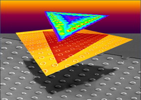 |
| Strain-tolerant, triangular, monolayer crystals of WS2 were grown on SiO2 substrates patterned with donut-shaped pillars, as shown in scanning electron microscope (bottom) and atomic force microscope (middle) image elements. The curvature of the pillars induced strain in the overlying crystals that locally altered their optoelectronic properties, as shown in bright regions of photoluminescence (top). CREDIT Christopher Rouleau/Oak Ridge National Laboratory, US Dept. of Energy |
Abstract:
A team led by scientists at the Department of Energy's Oak Ridge National Laboratory explored how atomically thin two-dimensional (2D) crystals can grow over 3D objects and how the curvature of those objects can stretch and strain the crystals. The findings, published in Science Advances, point to a strategy for engineering strain directly during the growth of atomically thin crystals to fabricate single photon emitters for quantum information processing.
2D crystals conforming to 3D curves create strain for engineering quantum devices
Oak Ridge, TN | Posted on June 7th, 2019The team first explored growth of the flat crystals on substrates patterned with sharp steps and trenches. Surprisingly, the crystals conformally grew up and down these flat obstacles without changing their properties or growth rates. However, curvy surfaces required the crystals to stretch as they grew to maintain their crystal structure. This growth of 2D crystals into the third dimension presented a fascinating opportunity.
"You can engineer how much strain you impart to a crystal by designing objects for them to grow over," said Kai Xiao, who with ORNL colleagues David Geohegan and postdoctoral researcher Kai Wang (now at Intel) conceived the study. "Strain is one way to make 'hot spots' for single photon emitters."
Conformal growth of perfect 2D crystals over 3D objects has the promise to localize strain to create high-fidelity arrays of single photon emitters. Stretching or compressing the crystal lattice changes the material's band gap, the energy gap between the valence and conduction bands of electrons, which largely determines a material's optoelectronic properties. Using strain engineering, researchers can funnel charge carriers to recombine precisely where desired in the crystal instead of at random defect locations. By tailoring curved objects to localize strain in the crystal, and then measuring resulting shifts in optical properties, the experimentalists compelled co-authors at Rice University--theorists Henry Yu, Nitant Gupta and Boris Yakobson--to simulate and map how curvature induces strain during crystal growth.
At ORNL, Wang and Xiao designed experiments with Bernadeta Srijanto to explore the growth of 2D crystals over lithographically patterned arrays of nanoscale shapes. Srijanto first used photolithography masks to protect certain areas of a silicon oxide surface during exposure to light, and then etched away the exposed surfaces to leave vertically standing shapes, including donuts, cones and steps. Wang and another postdoctoral researcher, Xufan Li (now at Honda Research Institute), then inserted the substrates into a furnace where vaporized tungsten oxide and sulfur reacted to deposit tungsten disulfide on the substrates as monolayer crystals. The crystals grew as an orderly lattice of atoms in perfect triangular tiles that grew larger with time by adding row after row of atoms to their outer edges. While the 2D crystals seemed to effortlessly fold like paper over tall steps and sharp trenches, growth over curved objects forced the crystals to stretch to maintain their triangular shape.
The scientists found that "donuts" 40 nanometers high were great candidates for single photon emitters because the crystals could reliably tolerate the strain they induced, and the maximum strain was precisely in the "hole" of the donut, as measured by shifts in the photoluminescence and Raman scattering. In the future, arrays of donuts or other structures could be patterned anywhere that quantum emitters are desired before the crystals are grown.
Wang and ORNL co-author Alex Puretzky used photoluminescence mapping to reveal where the crystals nucleated and how fast each edge of the triangular crystal progressed as it grew over the donuts. After careful analysis of the images, they were surprised to discover that although the crystals maintained their perfect shapes, the edges of crystals that had been strained by donuts grew faster.
To explain this acceleration, Puretzky developed a crystal growth model, and colleague Mina Yoon conducted first-principles calculations. Their work showed that strain is more likely to induce defects on the growing edge of a crystal. These defects can multiply the number of nucleation sites that seed crystal growth along an edge, allowing it to grow faster than before.
The reason crystals can grow easily up and down deep trenches, but become strained by shallow donuts, has to do with conformity and curvature. Imagine wrapping presents. Boxes are easy to wrap because the paper can fold to conform to the shape. But an irregularly shaped object with curves, such as an unboxed mug, is impossible to wrap conformally (to avoid tearing the paper, you would have to be able to stretch it like plastic wrap.)
The 2D crystals also stretch to conform to the substrate's curves. Eventually, however, the strain becomes too great and the crystals split to release the strain, atomic force microscopy and other techniques revealed. After the crystal cracks, growth of the still-strained material proceeds in different directions for each new arm. At Nanjing University of Aeronautics and Astronautics, Zhili Hu performed phase-field simulations of crystal branching. Xiang Gao of ORNL and Mengkun Tian (formerly of the University of Tennessee) analyzed the atomic structure of the crystals by scanning transmission electron microscopy.
"The results present exciting opportunities to take two-dimensional materials and vertically integrate them into the third dimension for next-generation electronics," said Xiao.
Next the researchers will explore whether strain can enhance the performance of tailored materials. "We're exploring how the strain of the crystal can make it easier to induce a phase change so the crystal can take on entirely new properties," Xiao said. "At the Center for Nanophase Materials Sciences, we're developing tools that will allow us to probe these structures and their quantum information aspects."
###
The title of the paper is "Strain tolerance of two-dimensional crystal growth on curved surfaces."
####
For more information, please click here
Contacts:
Dawn Levy
865-576-6448
Copyright © Oak Ridge National Laboratory
If you have a comment, please Contact us.Issuers of news releases, not 7th Wave, Inc. or Nanotechnology Now, are solely responsible for the accuracy of the content.
Bookmark:


| Related News Press |
News and information
![]() Quantum computer improves AI predictions April 17th, 2026
Quantum computer improves AI predictions April 17th, 2026
![]() Flexible sensor gains sensitivity under pressure April 17th, 2026
Flexible sensor gains sensitivity under pressure April 17th, 2026
![]() A reusable chip for particulate matter sensing April 17th, 2026
A reusable chip for particulate matter sensing April 17th, 2026
![]() Detecting vibrational quantum beating in the predissociation dynamics of SF6 using time-resolved photoelectron spectroscopy April 17th, 2026
Detecting vibrational quantum beating in the predissociation dynamics of SF6 using time-resolved photoelectron spectroscopy April 17th, 2026
2 Dimensional Materials
![]() Flexible sensor gains sensitivity under pressure April 17th, 2026
Flexible sensor gains sensitivity under pressure April 17th, 2026
![]() MXene nanomaterials enter a new dimension Multilayer nanomaterial: MXene flakes created at Drexel University show new promise as 1D scrolls January 30th, 2026
MXene nanomaterials enter a new dimension Multilayer nanomaterial: MXene flakes created at Drexel University show new promise as 1D scrolls January 30th, 2026
![]() ICFO researchers overcome long-standing bottleneck in single photon detection with twisted 2D materials August 8th, 2025
ICFO researchers overcome long-standing bottleneck in single photon detection with twisted 2D materials August 8th, 2025
![]() First real-time observation of two-dimensional melting process: Researchers at Mainz University unveil new insights into magnetic vortex structures August 8th, 2025
First real-time observation of two-dimensional melting process: Researchers at Mainz University unveil new insights into magnetic vortex structures August 8th, 2025
Imaging
![]() Simple algorithm paired with standard imaging tool could predict failure in lithium metal batteries August 8th, 2025
Simple algorithm paired with standard imaging tool could predict failure in lithium metal batteries August 8th, 2025
Laboratories
![]() Researchers develop molecular qubits that communicate at telecom frequencies October 3rd, 2025
Researchers develop molecular qubits that communicate at telecom frequencies October 3rd, 2025
Nanofabrication
![]() Self-propelled protein-based nanomotors for enhanced cancer therapy by inducing ferroptosis June 6th, 2025
Self-propelled protein-based nanomotors for enhanced cancer therapy by inducing ferroptosis June 6th, 2025
![]() Multiphoton polymerization: A promising technology for precision medicine February 28th, 2025
Multiphoton polymerization: A promising technology for precision medicine February 28th, 2025
Govt.-Legislation/Regulation/Funding/Policy
![]() Quantum computer improves AI predictions April 17th, 2026
Quantum computer improves AI predictions April 17th, 2026
![]() Metasurfaces smooth light to boost magnetic sensing precision January 30th, 2026
Metasurfaces smooth light to boost magnetic sensing precision January 30th, 2026
![]() New imaging approach transforms study of bacterial biofilms August 8th, 2025
New imaging approach transforms study of bacterial biofilms August 8th, 2025
Possible Futures
![]() A fundamentally new therapeutic approach to cystic fibrosis: Nanobody repairs cellular defect April 17th, 2026
A fundamentally new therapeutic approach to cystic fibrosis: Nanobody repairs cellular defect April 17th, 2026
![]() UC Irvine physicists discover method to reverse �quantum scrambling� : The work addresses the problem of information loss in quantum computing system April 17th, 2026
UC Irvine physicists discover method to reverse �quantum scrambling� : The work addresses the problem of information loss in quantum computing system April 17th, 2026
Discoveries
![]() Quantum computer improves AI predictions April 17th, 2026
Quantum computer improves AI predictions April 17th, 2026
![]() Flexible sensor gains sensitivity under pressure April 17th, 2026
Flexible sensor gains sensitivity under pressure April 17th, 2026
![]() A reusable chip for particulate matter sensing April 17th, 2026
A reusable chip for particulate matter sensing April 17th, 2026
![]() Detecting vibrational quantum beating in the predissociation dynamics of SF6 using time-resolved photoelectron spectroscopy April 17th, 2026
Detecting vibrational quantum beating in the predissociation dynamics of SF6 using time-resolved photoelectron spectroscopy April 17th, 2026
Interviews/Book Reviews/Essays/Reports/Podcasts/Journals/White papers/Posters
![]() A fundamentally new therapeutic approach to cystic fibrosis: Nanobody repairs cellular defect April 17th, 2026
A fundamentally new therapeutic approach to cystic fibrosis: Nanobody repairs cellular defect April 17th, 2026
![]() UC Irvine physicists discover method to reverse �quantum scrambling� : The work addresses the problem of information loss in quantum computing system April 17th, 2026
UC Irvine physicists discover method to reverse �quantum scrambling� : The work addresses the problem of information loss in quantum computing system April 17th, 2026
Tools
![]() Metasurfaces smooth light to boost magnetic sensing precision January 30th, 2026
Metasurfaces smooth light to boost magnetic sensing precision January 30th, 2026
![]() From sensors to smart systems: the rise of AI-driven photonic noses January 30th, 2026
From sensors to smart systems: the rise of AI-driven photonic noses January 30th, 2026
![]() Japan launches fully domestically produced quantum computer: Expo visitors to experience quantum computing firsthand August 8th, 2025
Japan launches fully domestically produced quantum computer: Expo visitors to experience quantum computing firsthand August 8th, 2025
Research partnerships
![]() Lab to industry: InSe wafer-scale breakthrough for future electronics August 8th, 2025
Lab to industry: InSe wafer-scale breakthrough for future electronics August 8th, 2025
![]() HKU physicists uncover hidden order in the quantum world through deconfined quantum critical points April 25th, 2025
HKU physicists uncover hidden order in the quantum world through deconfined quantum critical points April 25th, 2025
Quantum nanoscience
![]() Beyond silicon: Electronics at the scale of a single molecule January 30th, 2026
Beyond silicon: Electronics at the scale of a single molecule January 30th, 2026
![]() MXene nanomaterials enter a new dimension Multilayer nanomaterial: MXene flakes created at Drexel University show new promise as 1D scrolls January 30th, 2026
MXene nanomaterials enter a new dimension Multilayer nanomaterial: MXene flakes created at Drexel University show new promise as 1D scrolls January 30th, 2026
![]() ICFO researchers overcome long-standing bottleneck in single photon detection with twisted 2D materials August 8th, 2025
ICFO researchers overcome long-standing bottleneck in single photon detection with twisted 2D materials August 8th, 2025
|
|
||
|
|
||
| The latest news from around the world, FREE | ||
|
|
||
|
|
||
| Premium Products | ||
|
|
||
|
Only the news you want to read!
Learn More |
||
|
|
||
|
Full-service, expert consulting
Learn More |
||
|
|
||