Home > Press > Pushing Past Limits: Junkai Jiang receives prestigious Ph.D. Student Fellowship from IEEE Electron Devices Society
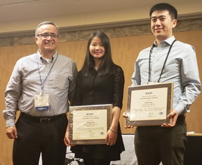 |
| Junkai Jiang, right, receives his award from IEEE EDS president D. Fernando Guarin, left, along with fellow recipient Yuanyuan Shi, a doctoral student in Spain |
Abstract:
The steady improvement of the performance and versatility of our electronic systems is due in large part to the scaling-down of transistors and interconnects that drive them. Components on the chips have been shrunk, stacked and more densely packed to add increased functionality without expanding the systems’ small footprints.
Pushing Past Limits: Junkai Jiang receives prestigious Ph.D. Student Fellowship from IEEE Electron Devices Society
Santa Barbara, CA | Posted on March 14th, 2019But the smaller, denser arrangements present their own set of challenges, and electronics engineers and designers everywhere are trying to find ways to overcome the resulting degradation in performance, reliability and energy efficiency.
UC Santa Barbara doctoral student Junkai Jiang is one of those people, and for his work he has been awarded a prestigious Ph.D. Student Fellowship from the Institute of Electrical and Electronics Engineers’ Electron Devices Society (EDS).
“The IEEE EDS Ph.D. Student Fellowship is one of the most prestigious awards for doctoral students working in the broad area of electron devices,” said UC Santa Barbara electrical and computer engineering professor Kaustav Banerjee, who is Jiang’s advisor. Junkai’s achievements in his research are certainly most deserving of this honor.”
A leader in the field of nanoelectronics, Banerjee is internationally recognized for his pioneering work on 2D materials and electronics. Jiang joined Banerjee’s Nanoelectronics Research Lab (NRL) in 2012 as a dual M.S./Ph.D. student after completing his bachelor of science degree in microelectronics at Peking University in China.
“I am extremely honored to receive this prestigious award from the IEEE Electron Devices Society that recognizes technological innovations by young Ph.D. student researchers,” Jiang said. “Being the only student from the entire Americas and the third student from the NRL at UC Santa Barbara to receive this award, I would like to especially thank my advisor, Professor Kaustav Banerjee, not only for his constant encouragement and support, but also for his inspirational guidance to identify and pursue cutting-edge research of the highest caliber, which helped me to progress steadily during the past several years of my doctoral research.”
Jiang’s work centers on interconnects — the conducting channels of electronic signal and power between and through components. Interconnects play a dominant role in determining the performance and power-dissipation of all integrated circuits, including state-of-the-art microprocessors. As the dimensions of on-chip components have scaled down and their number has increased, the conventional copper wire interconnects have also had to shrink, causing them to hit limits in terms of their ability to conduct signal and power rapidly, reliably and without interference. As a result, the systems may slow down, overheat and drain their batteries sooner than expected.
The answer to this problem could come in the form of graphene, a two-dimensional form of carbon with interesting and valuable electronic properties.
“My research is focused on designing and fabricating fast, energy-efficient and highly reliable on-chip interconnects and passives uniquely enabled by low-dimensional carbon nanomaterials such as graphene,” Jiang explained.
Graphene, with its atom-thick dimension and electronic conduction properties, has emerged as a viable replacement for copper wire interconnects primarily driven by Banerjee over the past decade. But its ability to revolutionize modern electronics is directly related to the ease of large-scale manufacture, which also is a thrust of Jiang’s research.
“Supported by this award, I have been working on integrating graphene in the high-volume-manufacturing friendly or ‘CMOS-compatible’ process and its application in demonstrating a multilayer VLSI (Very Large Scale Integrated Circuit) interconnect scheme to establish its feasibility for the semiconductor industry,” Jiang added.
“I offer sincere congratulations to Junkai Jiang for receiving this prestigious award, and to Professor Banerjee for the support that is indispensable to such achievement,” said Rod Alferness, dean of the UC Santa Barbara College of Engineering. “Given to only a single student in the Americas and only three in the world, this award is a major testament not only to Junkai, but also to the kind of students we attract at UCSB and the pioneering spirit they bring to tackling important problems.”
The IEEE Electron Devices Society Ph.D. Student Fellowship Award recognizes a demonstrated ability to perform independent research in the fields of electron devices and a proven history of academic excellence. Among Jiang’s other early-career accomplishments are receipt of the UCSB Graduate Division Dissertation award (2019) and the IEEE S3S Best Student Paper Award (2018). His research contributions have appeared in prestigious international journals, including Nature Electronics, Nano Letters and IEEE Transactions on Electron Devices, as well as leading IEEE conferences such as the annual International Electron Devices Meeting (IEDM) and the International Reliability Physics Symposium (IRPS).
To allow circuit level design and optimization, Jiang also developed a SPICE-compatible compact model for graphene interconnects, which was made available to the worldwide research community via nanoHUB, a well-known educational hub for the nanoelectronics community. His model currently has over 3000 users. In 2018, Jiang was one of the key contributors to the demonstration of the world’s first kinetic inductor, led by Banerjee, that overcame a 200-year old limitation of conventional inductors.
IEEE is the world’s largest technical professional organization for the advancement of technology. The Electron Devices Society (EDS), which began in 1952, is a technical society of the IEEE with more than 11,000 members worldwide.
####
For more information, please click here
Contacts:
Sonia Fernandez
(805) 893-4765
sonia(dot)fernandez(at)ucsb(dot)edu
Copyright © University of California, Santa Barbara
If you have a comment, please Contact us.Issuers of news releases, not 7th Wave, Inc. or Nanotechnology Now, are solely responsible for the accuracy of the content.
Bookmark:


| Related News Press |
News and information
![]() Quantum computer improves AI predictions April 17th, 2026
Quantum computer improves AI predictions April 17th, 2026
![]() Flexible sensor gains sensitivity under pressure April 17th, 2026
Flexible sensor gains sensitivity under pressure April 17th, 2026
![]() A reusable chip for particulate matter sensing April 17th, 2026
A reusable chip for particulate matter sensing April 17th, 2026
![]() Detecting vibrational quantum beating in the predissociation dynamics of SF6 using time-resolved photoelectron spectroscopy April 17th, 2026
Detecting vibrational quantum beating in the predissociation dynamics of SF6 using time-resolved photoelectron spectroscopy April 17th, 2026
Academic/Education
![]() Rice University launches Rice Synthetic Biology Institute to improve lives January 12th, 2024
Rice University launches Rice Synthetic Biology Institute to improve lives January 12th, 2024
![]() Multi-institution, $4.6 million NSF grant to fund nanotechnology training September 9th, 2022
Multi-institution, $4.6 million NSF grant to fund nanotechnology training September 9th, 2022
Chip Technology
![]() A reusable chip for particulate matter sensing April 17th, 2026
A reusable chip for particulate matter sensing April 17th, 2026
![]() Metasurfaces smooth light to boost magnetic sensing precision January 30th, 2026
Metasurfaces smooth light to boost magnetic sensing precision January 30th, 2026
Announcements
![]() A fundamentally new therapeutic approach to cystic fibrosis: Nanobody repairs cellular defect April 17th, 2026
A fundamentally new therapeutic approach to cystic fibrosis: Nanobody repairs cellular defect April 17th, 2026
![]() UC Irvine physicists discover method to reverse ‘quantum scrambling’ : The work addresses the problem of information loss in quantum computing system April 17th, 2026
UC Irvine physicists discover method to reverse ‘quantum scrambling’ : The work addresses the problem of information loss in quantum computing system April 17th, 2026
Grants/Sponsored Research/Awards/Scholarships/Gifts/Contests/Honors/Records
![]() Quantum computer improves AI predictions April 17th, 2026
Quantum computer improves AI predictions April 17th, 2026
![]() Detecting vibrational quantum beating in the predissociation dynamics of SF6 using time-resolved photoelectron spectroscopy April 17th, 2026
Detecting vibrational quantum beating in the predissociation dynamics of SF6 using time-resolved photoelectron spectroscopy April 17th, 2026
![]() Metasurfaces smooth light to boost magnetic sensing precision January 30th, 2026
Metasurfaces smooth light to boost magnetic sensing precision January 30th, 2026
|
|
||
|
|
||
| The latest news from around the world, FREE | ||
|
|
||
|
|
||
| Premium Products | ||
|
|
||
|
Only the news you want to read!
Learn More |
||
|
|
||
|
Full-service, expert consulting
Learn More |
||
|
|
||