Home > Press > When semiconductors stick together, materials go quantum: A new study led by Berkeley Lab reveals how aligned layers of atomically thin semiconductors can yield an exotic new quantum material
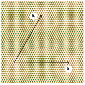 |
| The twist angle formed between atomically thin layers of tungsten disulfide and tungsten diselenide acts as a "tuning knob," turning ordinary semiconductors into an exotic quantum material. CREDIT Berkeley Lab |
Abstract:
A team of researchers led by the Department of Energy's Lawrence Berkeley National Laboratory (Berkeley Lab) has developed a simple method that could turn ordinary semiconducting materials into quantum machines - superthin devices marked by extraordinary electronic behavior. Such an advancement could help to revolutionize a number of industries aiming for energy-efficient electronic systems - and provide a platform for exotic new physics.
When semiconductors stick together, materials go quantum: A new study led by Berkeley Lab reveals how aligned layers of atomically thin semiconductors can yield an exotic new quantum material
Berkeley, CA | Posted on March 12th, 2019The study describing the method, which stacks together 2D layers of tungsten disulfide and tungsten diselenide to create an intricately patterned material, or superlattice, was published online recently in the journal Nature.
"This is an amazing discovery because we didn't think of these semiconducting materials as strongly interacting," said Feng Wang, a condensed matter physicist with Berkeley Lab's Materials Sciences Division and professor of physics at UC Berkeley. "Now this work has brought these seemingly ordinary semiconductors into the quantum materials space."
Two-dimensional (2D) materials, which are just one atom thick, are like nanosized building blocks that can be stacked arbitrarily to form tiny devices. When the lattices of two 2D materials are similar and well-aligned, a repeating pattern called a moir� superlattice can form.
For the past decade, researchers have been studying ways to combine different 2D materials, often starting with graphene - a material known for its ability to efficiently conduct heat and electricity. Out of this body of work, other researchers had discovered that moir� superlattices formed with graphene exhibit exotic physics such as superconductivity when the layers are aligned at just the right angle.
The new study, led by Wang, used 2D samples of semiconducting materials - tungsten disulfide and tungsten diselenide - to show that the twist angle between layers provides a "tuning knob" to turn a 2D semiconducting system into an exotic quantum material with highly interacting electrons.
Entering a new realm of physics
Co-lead authors Chenhao Jin, a postdoctoral scholar, and Emma Regan, a graduate student researcher, both of whom work under Wang in the Ultrafast Nano-Optics Group at UC Berkeley, fabricated the tungsten disulfide and tungsten diselenide samples using a polymer-based technique to pick up and transfer flakes of the materials, each measuring just tens of microns in diameter, into a stack.
They had fabricated similar samples of the materials for a previous study, but with the two layers stacked at no particular angle. When they measured the optical absorption of a new tungsten disulfide and tungsten diselenide sample for the current study, they were taken completely by surprise.
The absorption of visible light in a tungsten disulfide/tungsten diselenide device is largest when the light has the same energy as the system's exciton, a quasiparticle that consists of an electron bound to a hole that is common in 2D semiconductors. (In physics, a hole is a currently vacant state that an electron could occupy.)
For light in the energy range that the researchers were considering, they expected to see one peak in the signal that corresponded to the energy of an exciton.
Instead, they found that the original peak that they expected to see had split into three different peaks representing three distinct exciton states.
What could have increased the number of exciton states in the tungsten disulfide/tungsten device from one to three? Was it the addition of a moir� superlattice?
To find out, their collaborators Aiming Yan and Alex Zettl used a transmission electron microscope (TEM) at Berkeley Lab's Molecular Foundry, a nanoscale science research facility, to take atomic-resolution images of the tungsten disulfide/tungsten diselenide device to check how the materials' lattices were aligned.
The TEM images confirmed what they had suspected all along: the materials had indeed formed a moir� superlattice. "We saw beautiful, repeating patterns over the entire sample," said Regan. "After comparing this experimental observation with a theoretical model, we found that the moir� pattern introduces a large potential energy periodically over the device and could therefore introduce exotic quantum phenomena."
The researchers next plan to measure how this new quantum system could be applied to optoelectronics, which relates to the use of light in electronics; valleytronics, a field that could extend the limits of Moore's law by miniaturizing electronic components; and superconductivity, which would allow electrons to flow in devices with virtually no resistance.
###
Also contributing to the study were researchers from Arizona State University and the National Institute for Materials Science in Japan.
The work was supported by the DOE Office of Science. Additional funding was provided by the National Science Foundation, the Department of Defense, and the Elemental Strategy Initiative conducted by MEXT, Japan, and JSPS KAKENHI. The Molecular Foundry is a DOE Office of Science user facility.
####
About Lawrence Berkeley National Laboratory
Founded in 1931 on the belief that the biggest scientific challenges are best addressed by teams, Lawrence Berkeley National Laboratory and its scientists have been recognized with 13 Nobel Prizes. Today, Berkeley Lab researchers develop sustainable energy and environmental solutions, create useful new materials, advance the frontiers of computing, and probe the mysteries of life, matter, and the universe. Scientists from around the world rely on the Lab's facilities for their own discovery science. Berkeley Lab is a multiprogram national laboratory, managed by the University of California for the U.S. Department of Energy's Office of Science.
DOE's Office of Science is the single largest supporter of basic research in the physical sciences in the United States, and is working to address some of the most pressing challenges of our time. For more information, please visit science.energy.gov.
For more information, please click here
Contacts:
Theresa Duque
510-495-2418
Copyright © Lawrence Berkeley National Laboratory
If you have a comment, please Contact us.Issuers of news releases, not 7th Wave, Inc. or Nanotechnology Now, are solely responsible for the accuracy of the content.
Bookmark:


| Related Links |
| Related News Press |
News and information
![]() Quantum computer improves AI predictions April 17th, 2026
Quantum computer improves AI predictions April 17th, 2026
![]() Flexible sensor gains sensitivity under pressure April 17th, 2026
Flexible sensor gains sensitivity under pressure April 17th, 2026
![]() A reusable chip for particulate matter sensing April 17th, 2026
A reusable chip for particulate matter sensing April 17th, 2026
![]() Detecting vibrational quantum beating in the predissociation dynamics of SF6 using time-resolved photoelectron spectroscopy April 17th, 2026
Detecting vibrational quantum beating in the predissociation dynamics of SF6 using time-resolved photoelectron spectroscopy April 17th, 2026
Quantum Physics
![]() Detecting vibrational quantum beating in the predissociation dynamics of SF6 using time-resolved photoelectron spectroscopy April 17th, 2026
Detecting vibrational quantum beating in the predissociation dynamics of SF6 using time-resolved photoelectron spectroscopy April 17th, 2026
![]() Beyond silicon: Electronics at the scale of a single molecule January 30th, 2026
Beyond silicon: Electronics at the scale of a single molecule January 30th, 2026
Superconductivity
Govt.-Legislation/Regulation/Funding/Policy
![]() Quantum computer improves AI predictions April 17th, 2026
Quantum computer improves AI predictions April 17th, 2026
![]() Metasurfaces smooth light to boost magnetic sensing precision January 30th, 2026
Metasurfaces smooth light to boost magnetic sensing precision January 30th, 2026
![]() New imaging approach transforms study of bacterial biofilms August 8th, 2025
New imaging approach transforms study of bacterial biofilms August 8th, 2025
Possible Futures
![]() A fundamentally new therapeutic approach to cystic fibrosis: Nanobody repairs cellular defect April 17th, 2026
A fundamentally new therapeutic approach to cystic fibrosis: Nanobody repairs cellular defect April 17th, 2026
![]() UC Irvine physicists discover method to reverse �quantum scrambling� : The work addresses the problem of information loss in quantum computing system April 17th, 2026
UC Irvine physicists discover method to reverse �quantum scrambling� : The work addresses the problem of information loss in quantum computing system April 17th, 2026
Chip Technology
![]() A reusable chip for particulate matter sensing April 17th, 2026
A reusable chip for particulate matter sensing April 17th, 2026
![]() Metasurfaces smooth light to boost magnetic sensing precision January 30th, 2026
Metasurfaces smooth light to boost magnetic sensing precision January 30th, 2026
Optical computing/Photonic computing
![]() ICFO researchers overcome long-standing bottleneck in single photon detection with twisted 2D materials August 8th, 2025
ICFO researchers overcome long-standing bottleneck in single photon detection with twisted 2D materials August 8th, 2025
![]() Programmable electron-induced color router array May 14th, 2025
Programmable electron-induced color router array May 14th, 2025
Nanoelectronics
![]() Lab to industry: InSe wafer-scale breakthrough for future electronics August 8th, 2025
Lab to industry: InSe wafer-scale breakthrough for future electronics August 8th, 2025
![]() Interdisciplinary: Rice team tackles the future of semiconductors Multiferroics could be the key to ultralow-energy computing October 6th, 2023
Interdisciplinary: Rice team tackles the future of semiconductors Multiferroics could be the key to ultralow-energy computing October 6th, 2023
![]() Key element for a scalable quantum computer: Physicists from Forschungszentrum J�lich and RWTH Aachen University demonstrate electron transport on a quantum chip September 23rd, 2022
Key element for a scalable quantum computer: Physicists from Forschungszentrum J�lich and RWTH Aachen University demonstrate electron transport on a quantum chip September 23rd, 2022
![]() Reduced power consumption in semiconductor devices September 23rd, 2022
Reduced power consumption in semiconductor devices September 23rd, 2022
Discoveries
![]() Quantum computer improves AI predictions April 17th, 2026
Quantum computer improves AI predictions April 17th, 2026
![]() Flexible sensor gains sensitivity under pressure April 17th, 2026
Flexible sensor gains sensitivity under pressure April 17th, 2026
![]() A reusable chip for particulate matter sensing April 17th, 2026
A reusable chip for particulate matter sensing April 17th, 2026
![]() Detecting vibrational quantum beating in the predissociation dynamics of SF6 using time-resolved photoelectron spectroscopy April 17th, 2026
Detecting vibrational quantum beating in the predissociation dynamics of SF6 using time-resolved photoelectron spectroscopy April 17th, 2026
Announcements
![]() A fundamentally new therapeutic approach to cystic fibrosis: Nanobody repairs cellular defect April 17th, 2026
A fundamentally new therapeutic approach to cystic fibrosis: Nanobody repairs cellular defect April 17th, 2026
![]() UC Irvine physicists discover method to reverse �quantum scrambling� : The work addresses the problem of information loss in quantum computing system April 17th, 2026
UC Irvine physicists discover method to reverse �quantum scrambling� : The work addresses the problem of information loss in quantum computing system April 17th, 2026
Interviews/Book Reviews/Essays/Reports/Podcasts/Journals/White papers/Posters
![]() A fundamentally new therapeutic approach to cystic fibrosis: Nanobody repairs cellular defect April 17th, 2026
A fundamentally new therapeutic approach to cystic fibrosis: Nanobody repairs cellular defect April 17th, 2026
![]() UC Irvine physicists discover method to reverse �quantum scrambling� : The work addresses the problem of information loss in quantum computing system April 17th, 2026
UC Irvine physicists discover method to reverse �quantum scrambling� : The work addresses the problem of information loss in quantum computing system April 17th, 2026
Military
![]() Quantum engineers �squeeze� laser frequency combs to make more sensitive gas sensors January 17th, 2025
Quantum engineers �squeeze� laser frequency combs to make more sensitive gas sensors January 17th, 2025
![]() Chainmail-like material could be the future of armor: First 2D mechanically interlocked polymer exhibits exceptional flexibility and strength January 17th, 2025
Chainmail-like material could be the future of armor: First 2D mechanically interlocked polymer exhibits exceptional flexibility and strength January 17th, 2025
![]() Single atoms show their true color July 5th, 2024
Single atoms show their true color July 5th, 2024
![]() NRL charters Navy�s quantum inertial navigation path to reduce drift April 5th, 2024
NRL charters Navy�s quantum inertial navigation path to reduce drift April 5th, 2024
Grants/Sponsored Research/Awards/Scholarships/Gifts/Contests/Honors/Records
![]() Quantum computer improves AI predictions April 17th, 2026
Quantum computer improves AI predictions April 17th, 2026
![]() Detecting vibrational quantum beating in the predissociation dynamics of SF6 using time-resolved photoelectron spectroscopy April 17th, 2026
Detecting vibrational quantum beating in the predissociation dynamics of SF6 using time-resolved photoelectron spectroscopy April 17th, 2026
![]() Metasurfaces smooth light to boost magnetic sensing precision January 30th, 2026
Metasurfaces smooth light to boost magnetic sensing precision January 30th, 2026
Research partnerships
![]() Lab to industry: InSe wafer-scale breakthrough for future electronics August 8th, 2025
Lab to industry: InSe wafer-scale breakthrough for future electronics August 8th, 2025
![]() HKU physicists uncover hidden order in the quantum world through deconfined quantum critical points April 25th, 2025
HKU physicists uncover hidden order in the quantum world through deconfined quantum critical points April 25th, 2025
Quantum nanoscience
![]() Beyond silicon: Electronics at the scale of a single molecule January 30th, 2026
Beyond silicon: Electronics at the scale of a single molecule January 30th, 2026
![]() MXene nanomaterials enter a new dimension Multilayer nanomaterial: MXene flakes created at Drexel University show new promise as 1D scrolls January 30th, 2026
MXene nanomaterials enter a new dimension Multilayer nanomaterial: MXene flakes created at Drexel University show new promise as 1D scrolls January 30th, 2026
![]() ICFO researchers overcome long-standing bottleneck in single photon detection with twisted 2D materials August 8th, 2025
ICFO researchers overcome long-standing bottleneck in single photon detection with twisted 2D materials August 8th, 2025
|
|
||
|
|
||
| The latest news from around the world, FREE | ||
|
|
||
|
|
||
| Premium Products | ||
|
|
||
|
Only the news you want to read!
Learn More |
||
|
|
||
|
Full-service, expert consulting
Learn More |
||
|
|
||