Home > Press > The moirť patterns of three layers change the electronic properties of graphene
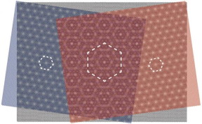 |
| A graphene layer (black) of hexagonally arranged carbon atoms is placed between two layers of boron nitride atoms, which are also arranged hexagonally with a slightly different size. The overlap creates honeycomb patterns in various sizes. CREDIT Swiss Nanoscience Institute, University of Basel |
Abstract:
Combining an atomically thin graphene and a boron nitride layer at a slightly rotated angle changes their electrical properties. Physicists at the University of Basel have now shown for the first time the combination with a third layer can result in new material properties also in a three-layer sandwich of carbon and boron nitride. This significantly increases the number of potential synthetic materials, report the researchers in the scientific journal Nano Letters.
The moirť patterns of three layers change the electronic properties of graphene
Basel, Switzerland | Posted on March 8th, 2019Last year, researchers in the US caused a big stir when they showed that rotating two stacked graphene layers by a "magical" angle of 1.1 degrees turns graphene superconducting - a striking example of how the combination of atomically thin materials can produce completely new electrical properties.
Precision alignment
Scientists from the Swiss Nanoscience Institute and the Department of Physics at the University of Basel have now taken this concept one step further. They placed a layer of graphene between two boron nitride layers, which is often serves to protect the sensitive carbon structure. Doing so, they aligned the layers very precisely with the crystal lattice of the graphene.
The effect observed by the physicists in Professor Christian SchŲnenberger's team is commonly known as a moirť pattern: when two regular patterns are superimposed, a new pattern results with a larger periodic lattice.
New three-layer superlattice
Lujun Wang, a member of the SNI PhD School and researcher in SchŲnenberger's team, also observed effects of this kind of superlattice when he combined layers of boron nitride and graphene. The atoms are arranged hexagonally in all layers. If they are stacked on top of each other, larger regular patterns emerge, with a size depending on the angle between the layers.
It had already been shown that this works with a two-layer combination of graphene and boron nitride, but the effects due to a second boron nitride layer had not yet been found.
When the physicists from Basel experimented with three layers, two superlattices were formed between the graphene and the upper and the lower boron nitride layer, respectively. The superposition of all three layers created an even larger superstructure than possible with only one layer.
Scientists are very interested in these types of synthetic materials, since the different moirť patterns can be used to change or artificially produce new electronic material properties.
"To put it simply, the atomic patterns determine the behavior of electrons in a material, and we are combining different naturally occurring patterns to create new synthetic materials," explains Dr. Andreas Baumgartner, who supervised the project. "Now we have discovered effects in these tailor-made electronic devices that are consistent with a three-layer superstructure," he adds.
####
For more information, please click here
Contacts:
Ylenia Sartorel
@UniBasel_en
Copyright © University of Basel
If you have a comment, please Contact us.Issuers of news releases, not 7th Wave, Inc. or Nanotechnology Now, are solely responsible for the accuracy of the content.
Bookmark:


| Related Links |
| Related News Press |
News and information
![]() Quantum computer improves AI predictions April 17th, 2026
Quantum computer improves AI predictions April 17th, 2026
![]() Flexible sensor gains sensitivity under pressure April 17th, 2026
Flexible sensor gains sensitivity under pressure April 17th, 2026
![]() A reusable chip for particulate matter sensing April 17th, 2026
A reusable chip for particulate matter sensing April 17th, 2026
![]() Detecting vibrational quantum beating in the predissociation dynamics of SF6 using time-resolved photoelectron spectroscopy April 17th, 2026
Detecting vibrational quantum beating in the predissociation dynamics of SF6 using time-resolved photoelectron spectroscopy April 17th, 2026
2 Dimensional Materials
![]() Flexible sensor gains sensitivity under pressure April 17th, 2026
Flexible sensor gains sensitivity under pressure April 17th, 2026
![]() MXene nanomaterials enter a new dimension Multilayer nanomaterial: MXene flakes created at Drexel University show new promise as 1D scrolls January 30th, 2026
MXene nanomaterials enter a new dimension Multilayer nanomaterial: MXene flakes created at Drexel University show new promise as 1D scrolls January 30th, 2026
![]() ICFO researchers overcome long-standing bottleneck in single photon detection with twisted 2D materials August 8th, 2025
ICFO researchers overcome long-standing bottleneck in single photon detection with twisted 2D materials August 8th, 2025
![]() First real-time observation of two-dimensional melting process: Researchers at Mainz University unveil new insights into magnetic vortex structures August 8th, 2025
First real-time observation of two-dimensional melting process: Researchers at Mainz University unveil new insights into magnetic vortex structures August 8th, 2025
![]() Lab to industry: InSe wafer-scale breakthrough for future electronics August 8th, 2025
Lab to industry: InSe wafer-scale breakthrough for future electronics August 8th, 2025
Superconductivity
![]() MXene nanomaterials enter a new dimension Multilayer nanomaterial: MXene flakes created at Drexel University show new promise as 1D scrolls January 30th, 2026
MXene nanomaterials enter a new dimension Multilayer nanomaterial: MXene flakes created at Drexel University show new promise as 1D scrolls January 30th, 2026
![]() Lattice-driven charge density wave fluctuations far above the transition temperature in Kagome superconductor April 25th, 2025
Lattice-driven charge density wave fluctuations far above the transition temperature in Kagome superconductor April 25th, 2025
Videos/Movies
![]() ICFO researchers overcome long-standing bottleneck in single photon detection with twisted 2D materials August 8th, 2025
ICFO researchers overcome long-standing bottleneck in single photon detection with twisted 2D materials August 8th, 2025
Graphene/ Graphite
![]() Electrifying results shed light on graphene foam as a potential material for lab grown cartilage June 6th, 2025
Electrifying results shed light on graphene foam as a potential material for lab grown cartilage June 6th, 2025
Possible Futures
![]() A fundamentally new therapeutic approach to cystic fibrosis: Nanobody repairs cellular defect April 17th, 2026
A fundamentally new therapeutic approach to cystic fibrosis: Nanobody repairs cellular defect April 17th, 2026
![]() UC Irvine physicists discover method to reverse Ďquantum scramblingí : The work addresses the problem of information loss in quantum computing system April 17th, 2026
UC Irvine physicists discover method to reverse Ďquantum scramblingí : The work addresses the problem of information loss in quantum computing system April 17th, 2026
Chip Technology
![]() A reusable chip for particulate matter sensing April 17th, 2026
A reusable chip for particulate matter sensing April 17th, 2026
![]() Metasurfaces smooth light to boost magnetic sensing precision January 30th, 2026
Metasurfaces smooth light to boost magnetic sensing precision January 30th, 2026
Discoveries
![]() Quantum computer improves AI predictions April 17th, 2026
Quantum computer improves AI predictions April 17th, 2026
![]() Flexible sensor gains sensitivity under pressure April 17th, 2026
Flexible sensor gains sensitivity under pressure April 17th, 2026
![]() A reusable chip for particulate matter sensing April 17th, 2026
A reusable chip for particulate matter sensing April 17th, 2026
![]() Detecting vibrational quantum beating in the predissociation dynamics of SF6 using time-resolved photoelectron spectroscopy April 17th, 2026
Detecting vibrational quantum beating in the predissociation dynamics of SF6 using time-resolved photoelectron spectroscopy April 17th, 2026
Announcements
![]() A fundamentally new therapeutic approach to cystic fibrosis: Nanobody repairs cellular defect April 17th, 2026
A fundamentally new therapeutic approach to cystic fibrosis: Nanobody repairs cellular defect April 17th, 2026
![]() UC Irvine physicists discover method to reverse Ďquantum scramblingí : The work addresses the problem of information loss in quantum computing system April 17th, 2026
UC Irvine physicists discover method to reverse Ďquantum scramblingí : The work addresses the problem of information loss in quantum computing system April 17th, 2026
Interviews/Book Reviews/Essays/Reports/Podcasts/Journals/White papers/Posters
![]() A fundamentally new therapeutic approach to cystic fibrosis: Nanobody repairs cellular defect April 17th, 2026
A fundamentally new therapeutic approach to cystic fibrosis: Nanobody repairs cellular defect April 17th, 2026
![]() UC Irvine physicists discover method to reverse Ďquantum scramblingí : The work addresses the problem of information loss in quantum computing system April 17th, 2026
UC Irvine physicists discover method to reverse Ďquantum scramblingí : The work addresses the problem of information loss in quantum computing system April 17th, 2026
|
|
||
|
|
||
| The latest news from around the world, FREE | ||
|
|
||
|
|
||
| Premium Products | ||
|
|
||
|
Only the news you want to read!
Learn More |
||
|
|
||
|
Full-service, expert consulting
Learn More |
||
|
|
||