Home > Press > Scientists image conducting edges in a promising 2-D material
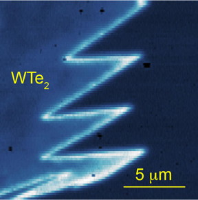 |
| The bright zigzag lines indicate conduction features precisely at the edges of the monolayer WTe2. (Cui Lab/UC Riverside) |
Abstract:
A research team comprised of scientists at the University of California, Riverside, and the University of Washington has for the first time directly imaged “edge conduction” in monolayer tungsten ditelluride, or WTe2, a newly discovered 2-D topological insulator and quantum material.
Scientists image conducting edges in a promising 2-D material
Riverside, CA | Posted on February 8th, 2019The research makes it possible to exploit this edge conduction feature to build more energy-efficient electronic devices.
In a typical conductor, electrical current flows everywhere. Insulators, on the other hand, do not readily conduct electricity. In topological insulators, a special type of material, the interior works as an insulator, but the boundaries of such materials are guaranteed to be conductive due to its topological property, resulting in a feature called “topological edge conduction.”
Topology is the mathematical study of the properties of a geometric figure or solid that is unchanged by stretching or bending. Applying this concept to electronic materials leads to discoveries of many interesting phenomena, including topological edge conduction. Working like highways for electrons, channels of topological edge conduction allow electrons to travel with little resistance. Further, because edge channels can be potentially very narrow, electronic devices can be further miniaturized.
Study results appear today in Science Advances.
“Several materials have been shown to be 3-D topological insulators,” said Yongtao Cui, an assistant professor of physics and astronomy at UCR, who led the research. “But 2-D topological insulators are rare. Several recent experiments established that monolayer WTe2 is the first atomically thin 2-D topological insulator.”
Cui explained that for a 3-D topological insulator, conduction appears at its surfaces; for a 2-D sheet-like material, such conducting features are simply at the edges of the sheet.
Cui’s lab used a novel experimental technique called Microwave Impedance Microscopy, or MIM, to directly image the conduction at the edges of monolayer WTe2.
“Our results unambiguously confirm edge conduction in this promising material,” Cui said.
Although WTe2 has been known to exist for decades, interest in this material got a boost in only the last few years due to its exotic physical and electronic properties discovered using topological physics. WTe2 layers are stacked together via van der Waals interactions and can be easily exfoliated into thin, 2-D, graphene-like sheets.
“In addition to conduction at the edges in monolayer WTe2, we also found that the conductive channels can extend to the interior of the material, due to imperfections — such as cracks,” Cui said. “Our observations point to new ways to control and engineer such conduction channels via mechanical or chemical means.”
Cui’s collaborators at the University of Washington prepared the monolayer WTe2 samples. At UCR, his lab performed the MIM measurement, which involved sending a microwave electrical signal to a sharp metal tip, and positioning the tip near the surface of monolayer WTe2. By resolving the microwave signal bounced back by the sample, the researchers could determine whether the sample region directly below the tip was conductive or not.
“We scanned the tip across the entire sample and directly mapped the local conductivity,” Cui said. “We performed all the measurements at cryogenic temperatures, needed for monolayer WTe2 to exhibit the topological property. The topological properties of monolayer WTe2 can potentially serve as a platform to realize essential operations in quantum computing.”
Cui’s lab is already exploring new ways to manipulate the edge conduction channels and topological physics in monolayer WTe2.
“We are looking into whether stacking monolayer WTe2 with other 2-D materials can alter its topological property,” he said. “We are also using mechanical and chemical methods to create networks of conduction channels. The MIM technique we used offers a powerful means to characterize the conduction channels in topological materials such as monolayer WTe2.”
Cui was joined in the study by Yanmeng Shi, Ben Niu, and Brian A. Francisco of UCR; Joshua Kahn, Zaiyao Fei, Bosong Sun, Xinghan Cai, Xiaodong Xu, and David H. Cobden of the University of Washington; Di Wu of Nanjing University, China; and Zhi-Xun Shen of Stanford University; Shi, Kahn, and Niu are co-first authors of the research paper.
The work done at UCR was supported by Cui’s startup funds.
####
About University of California - Riverside
The University of California, Riverside (www.ucr.edu) is a doctoral research university, a living laboratory for groundbreaking exploration of issues critical to Inland Southern California, the state and communities around the world. Reflecting California's diverse culture, UCR's enrollment is more than 24,000 students. The campus opened a medical school in 2013 and has reached the heart of the Coachella Valley by way of the UCR Palm Desert Center. The campus has an annual statewide economic impact of almost $2 billion. To learn more, email
For more information, please click here
Contacts:
Iqbal Pittalwala
(951) 827-6050
@UCR_Sciencenews
Copyright © University of California - Riverside
If you have a comment, please Contact us.Issuers of news releases, not 7th Wave, Inc. or Nanotechnology Now, are solely responsible for the accuracy of the content.
Bookmark:


| Related News Press |
News and information
![]() Quantum computer improves AI predictions April 17th, 2026
Quantum computer improves AI predictions April 17th, 2026
![]() Flexible sensor gains sensitivity under pressure April 17th, 2026
Flexible sensor gains sensitivity under pressure April 17th, 2026
![]() A reusable chip for particulate matter sensing April 17th, 2026
A reusable chip for particulate matter sensing April 17th, 2026
![]() Detecting vibrational quantum beating in the predissociation dynamics of SF6 using time-resolved photoelectron spectroscopy April 17th, 2026
Detecting vibrational quantum beating in the predissociation dynamics of SF6 using time-resolved photoelectron spectroscopy April 17th, 2026
2 Dimensional Materials
![]() Flexible sensor gains sensitivity under pressure April 17th, 2026
Flexible sensor gains sensitivity under pressure April 17th, 2026
![]() MXene nanomaterials enter a new dimension Multilayer nanomaterial: MXene flakes created at Drexel University show new promise as 1D scrolls January 30th, 2026
MXene nanomaterials enter a new dimension Multilayer nanomaterial: MXene flakes created at Drexel University show new promise as 1D scrolls January 30th, 2026
Imaging
Graphene/ Graphite
![]() Electrifying results shed light on graphene foam as a potential material for lab grown cartilage June 6th, 2025
Electrifying results shed light on graphene foam as a potential material for lab grown cartilage June 6th, 2025
![]() Breakthrough in proton barrier films using pore-free graphene oxide: Kumamoto University researchers achieve new milestone in advanced coating technologies September 13th, 2024
Breakthrough in proton barrier films using pore-free graphene oxide: Kumamoto University researchers achieve new milestone in advanced coating technologies September 13th, 2024
Possible Futures
![]() A fundamentally new therapeutic approach to cystic fibrosis: Nanobody repairs cellular defect April 17th, 2026
A fundamentally new therapeutic approach to cystic fibrosis: Nanobody repairs cellular defect April 17th, 2026
![]() UC Irvine physicists discover method to reverse ‘quantum scrambling’ : The work addresses the problem of information loss in quantum computing system April 17th, 2026
UC Irvine physicists discover method to reverse ‘quantum scrambling’ : The work addresses the problem of information loss in quantum computing system April 17th, 2026
Chip Technology
![]() A reusable chip for particulate matter sensing April 17th, 2026
A reusable chip for particulate matter sensing April 17th, 2026
![]() Metasurfaces smooth light to boost magnetic sensing precision January 30th, 2026
Metasurfaces smooth light to boost magnetic sensing precision January 30th, 2026
Discoveries
![]() Quantum computer improves AI predictions April 17th, 2026
Quantum computer improves AI predictions April 17th, 2026
![]() Flexible sensor gains sensitivity under pressure April 17th, 2026
Flexible sensor gains sensitivity under pressure April 17th, 2026
![]() A reusable chip for particulate matter sensing April 17th, 2026
A reusable chip for particulate matter sensing April 17th, 2026
![]() Detecting vibrational quantum beating in the predissociation dynamics of SF6 using time-resolved photoelectron spectroscopy April 17th, 2026
Detecting vibrational quantum beating in the predissociation dynamics of SF6 using time-resolved photoelectron spectroscopy April 17th, 2026
Materials/Metamaterials/Magnetoresistance
![]() First real-time observation of two-dimensional melting process: Researchers at Mainz University unveil new insights into magnetic vortex structures August 8th, 2025
First real-time observation of two-dimensional melting process: Researchers at Mainz University unveil new insights into magnetic vortex structures August 8th, 2025
![]() Researchers unveil a groundbreaking clay-based solution to capture carbon dioxide and combat climate change June 6th, 2025
Researchers unveil a groundbreaking clay-based solution to capture carbon dioxide and combat climate change June 6th, 2025
![]() A 1960s idea inspires NBI researchers to study hitherto inaccessible quantum states June 6th, 2025
A 1960s idea inspires NBI researchers to study hitherto inaccessible quantum states June 6th, 2025
![]() Institute for Nanoscience hosts annual proposal planning meeting May 16th, 2025
Institute for Nanoscience hosts annual proposal planning meeting May 16th, 2025
Announcements
![]() A fundamentally new therapeutic approach to cystic fibrosis: Nanobody repairs cellular defect April 17th, 2026
A fundamentally new therapeutic approach to cystic fibrosis: Nanobody repairs cellular defect April 17th, 2026
![]() UC Irvine physicists discover method to reverse ‘quantum scrambling’ : The work addresses the problem of information loss in quantum computing system April 17th, 2026
UC Irvine physicists discover method to reverse ‘quantum scrambling’ : The work addresses the problem of information loss in quantum computing system April 17th, 2026
Interviews/Book Reviews/Essays/Reports/Podcasts/Journals/White papers/Posters
![]() A fundamentally new therapeutic approach to cystic fibrosis: Nanobody repairs cellular defect April 17th, 2026
A fundamentally new therapeutic approach to cystic fibrosis: Nanobody repairs cellular defect April 17th, 2026
![]() UC Irvine physicists discover method to reverse ‘quantum scrambling’ : The work addresses the problem of information loss in quantum computing system April 17th, 2026
UC Irvine physicists discover method to reverse ‘quantum scrambling’ : The work addresses the problem of information loss in quantum computing system April 17th, 2026
Tools
![]() Metasurfaces smooth light to boost magnetic sensing precision January 30th, 2026
Metasurfaces smooth light to boost magnetic sensing precision January 30th, 2026
![]() From sensors to smart systems: the rise of AI-driven photonic noses January 30th, 2026
From sensors to smart systems: the rise of AI-driven photonic noses January 30th, 2026
![]() Japan launches fully domestically produced quantum computer: Expo visitors to experience quantum computing firsthand August 8th, 2025
Japan launches fully domestically produced quantum computer: Expo visitors to experience quantum computing firsthand August 8th, 2025
Research partnerships
![]() Lab to industry: InSe wafer-scale breakthrough for future electronics August 8th, 2025
Lab to industry: InSe wafer-scale breakthrough for future electronics August 8th, 2025
![]() HKU physicists uncover hidden order in the quantum world through deconfined quantum critical points April 25th, 2025
HKU physicists uncover hidden order in the quantum world through deconfined quantum critical points April 25th, 2025
Quantum nanoscience
![]() Beyond silicon: Electronics at the scale of a single molecule January 30th, 2026
Beyond silicon: Electronics at the scale of a single molecule January 30th, 2026
![]() MXene nanomaterials enter a new dimension Multilayer nanomaterial: MXene flakes created at Drexel University show new promise as 1D scrolls January 30th, 2026
MXene nanomaterials enter a new dimension Multilayer nanomaterial: MXene flakes created at Drexel University show new promise as 1D scrolls January 30th, 2026
![]() ICFO researchers overcome long-standing bottleneck in single photon detection with twisted 2D materials August 8th, 2025
ICFO researchers overcome long-standing bottleneck in single photon detection with twisted 2D materials August 8th, 2025
|
|
||
|
|
||
| The latest news from around the world, FREE | ||
|
|
||
|
|
||
| Premium Products | ||
|
|
||
|
Only the news you want to read!
Learn More |
||
|
|
||
|
Full-service, expert consulting
Learn More |
||
|
|
||