Home > Press > Novel method to fabricate nanoribbons from speeding nano droplets
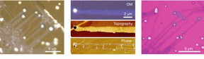 |
| From left are 1) Optical images of MoS2 ribbons grown on a NaCl crystal, 2) Optical microscopy (OM) and corresponding AFM topography and phase images of a ribbon, and 3) Optical image of the ribbons transferred onto a SiO2/Si substrate. CREDIT UNIST |
Abstract:
An international team of researchers, affiliated with UNIST has discovered a novel method for the synthesis of ultrathin semiconductors. This is a unique growth mechanism, which yielded nanoscopic semiconductor ribbons that are only a few atoms thick.
Novel method to fabricate nanoribbons from speeding nano droplets
Ulsan, Korea | Posted on May 29th, 2018This breakthrough has been jointly conducted by Distinguished Professor Feng Ding and Dr. Wen Zhao from the Center for Multidimensional Carbon Materials (CMCM), within the Institute for Basic Science (IBS) at UNIST, in collaboration with the National University of Singapore (NUS), the National Institute for Materials Science (NIMS), the National Institute of Advanced Industrial Science and Technology (AIST), and Shenzhen University.
In the study, the research team has successfully fabricated MoS2 nanoribbons via vapour-liquid-solid (VLS) growth mechanism, a type of chemical vapour deposition (CVD) process.
"Synthesis of vertically elongated structure via VLS growth mechanism."
Chemical vapor deposition or CVD is a generic name for a group of processes whereby a solid material is deposited from a vapor by a chemical reaction occurring on or in the vicinity of a normally heated substrate surface. It is the most widely adopted industrial techniques for producing semiconducting thin films and nanostructures.
"The range of structures that can be controllably synthesized by the current methods is still limited in terms of morphology, spatial selectivity, crystal orientation, layer number and chemical composition," the research team noted. "Therefore, developing versatile growth methods is essential to the realization of highly integrated electronic and photonic devices based on these materials.
"The current CVD-based growth process relies on the inherent dynamics of the precursors to diffuse and self-organize on the substrate surface, which results in crystallites with characteristic triangular or hexagonal shapes," says Dr. Zhao. "This unique growth mechanism of the nanoscopic semiconductor ribbons that are only a few atoms thick is an exciting discovery." In the study, she performed density functional theory based molecular dynamic (DFT-MD) simulations of the MoS2 precipitation process.
The proposed mechanism of VLS growth differs from commonly known CVD technique, as it involves the precursors introduced in the vapour phase form a liquid droplet intermediate before condensing into a solid product.
The team noted that the morphology of the growth product was, however, unlike what is normally expected from a VLS growth, which typically yields cylindrical or tubular structures rather than ribbons. Their observation suggests that the liquid droplet migrates on the substrate surface in a rather ordered manner, leaving behind a track of ultrathin crystal.
"Because the liquid droplet migrates on the substrate surface in a rather ordered manner, the morphology of the growth product yielded cylindrical or tubular structures rather than ribbons." says Dr. Zhao.
This time, however, the horizontal growth of predominantly monolayer MoS2 ribbons was obtained via VLS growth, a unique growth mechanism that has not been reported until now.
Their observation revealed that the VLS growth of monolayer MoS2 is triggered by the reaction between MoO3 and NaCl, which results in the formation of molten Na-Mo-O droplets. These droplets mediate the growth of MoS2 ribbons in the 'crawling mode' when saturated with sulfur. The locally well-defined orientations of the ribbons reveal the regular horizontal motion of the droplets during growth.
"Assisting the growth of MoS2 ribbons, like painting with a an ink droplet."
In order to gain insight into the liquid-solid transformation, Professor Ding's team performed density functional theory based molecular dynamic (DFT-MD) sumulations of the precipitation process. The simulation showed the attachment of molybdenum (Mo) and sulfur (S) to the previously established MoS2.
"It is worth noting that MoS2 is not oxidized despite the presence of large numbers of oxygen atoms," says the research team. "We also observe the nucleation of MoS2 clusters in regions that are rich in Mo and S atoms, further supporting the feasibility of liquid-mediated nucleation and growth of MoS2."
"This study has prompted questions about surface and interface growth of nanomaterials," says Professor Ding. "By identifying a suitable liquid-phase intermediate compound, we believe that it will be possible to realize the direct 1D growth of a range of van der Waals layered materials."
The team anticipates that many other materials can be grown using a similar approach. Their short-term goal is to understand the growth mechanism better and to control the morphology of the ribbons.
"Our work identified many interesting questions about surface and interface growth of nanomaterials," says Professor Goki Eda at the National University of Singapore (NUS), the corresponding author of this study. "We predict that the ability to directly grow complex structures will greatly facilitate the realization of high performance nanoelectronic circuits."
The team noted that their results provide insight into the distinct VLS growth mode of 2D MoS2 and demonstrate the potential of their implementation in nanoelectronic devices. The findings of this study have been published in the prestigious journal, Nature Materials on April 23, 2018.
####
For more information, please click here
Contacts:
JooHyeon Heo
82-522-171-223
Copyright © Ulsan National Institute of Science and Technology (UNIST)
If you have a comment, please Contact us.Issuers of news releases, not 7th Wave, Inc. or Nanotechnology Now, are solely responsible for the accuracy of the content.
Bookmark:


| Related Links |
| Related News Press |
News and information
![]() Quantum computer improves AI predictions April 17th, 2026
Quantum computer improves AI predictions April 17th, 2026
![]() Flexible sensor gains sensitivity under pressure April 17th, 2026
Flexible sensor gains sensitivity under pressure April 17th, 2026
![]() A reusable chip for particulate matter sensing April 17th, 2026
A reusable chip for particulate matter sensing April 17th, 2026
![]() Detecting vibrational quantum beating in the predissociation dynamics of SF6 using time-resolved photoelectron spectroscopy April 17th, 2026
Detecting vibrational quantum beating in the predissociation dynamics of SF6 using time-resolved photoelectron spectroscopy April 17th, 2026
2 Dimensional Materials
![]() Flexible sensor gains sensitivity under pressure April 17th, 2026
Flexible sensor gains sensitivity under pressure April 17th, 2026
Hardware
![]() The present and future of computing get a boost from new research July 21st, 2023
The present and future of computing get a boost from new research July 21st, 2023
![]() A Carbon Nanotube Microprocessor Mature Enough to Say Hello: Three new breakthroughs make commercial nanotube processors possible March 2nd, 2020
A Carbon Nanotube Microprocessor Mature Enough to Say Hello: Three new breakthroughs make commercial nanotube processors possible March 2nd, 2020
![]() Powering the future: Smallest all-digital circuit opens doors to 5 nm next-gen semiconductor February 11th, 2020
Powering the future: Smallest all-digital circuit opens doors to 5 nm next-gen semiconductor February 11th, 2020
Possible Futures
![]() A fundamentally new therapeutic approach to cystic fibrosis: Nanobody repairs cellular defect April 17th, 2026
A fundamentally new therapeutic approach to cystic fibrosis: Nanobody repairs cellular defect April 17th, 2026
![]() UC Irvine physicists discover method to reverse �quantum scrambling� : The work addresses the problem of information loss in quantum computing system April 17th, 2026
UC Irvine physicists discover method to reverse �quantum scrambling� : The work addresses the problem of information loss in quantum computing system April 17th, 2026
Chip Technology
![]() A reusable chip for particulate matter sensing April 17th, 2026
A reusable chip for particulate matter sensing April 17th, 2026
![]() Metasurfaces smooth light to boost magnetic sensing precision January 30th, 2026
Metasurfaces smooth light to boost magnetic sensing precision January 30th, 2026
Nanoelectronics
![]() Lab to industry: InSe wafer-scale breakthrough for future electronics August 8th, 2025
Lab to industry: InSe wafer-scale breakthrough for future electronics August 8th, 2025
![]() Interdisciplinary: Rice team tackles the future of semiconductors Multiferroics could be the key to ultralow-energy computing October 6th, 2023
Interdisciplinary: Rice team tackles the future of semiconductors Multiferroics could be the key to ultralow-energy computing October 6th, 2023
![]() Key element for a scalable quantum computer: Physicists from Forschungszentrum J�lich and RWTH Aachen University demonstrate electron transport on a quantum chip September 23rd, 2022
Key element for a scalable quantum computer: Physicists from Forschungszentrum J�lich and RWTH Aachen University demonstrate electron transport on a quantum chip September 23rd, 2022
![]() Reduced power consumption in semiconductor devices September 23rd, 2022
Reduced power consumption in semiconductor devices September 23rd, 2022
Discoveries
![]() Quantum computer improves AI predictions April 17th, 2026
Quantum computer improves AI predictions April 17th, 2026
![]() Flexible sensor gains sensitivity under pressure April 17th, 2026
Flexible sensor gains sensitivity under pressure April 17th, 2026
![]() A reusable chip for particulate matter sensing April 17th, 2026
A reusable chip for particulate matter sensing April 17th, 2026
![]() Detecting vibrational quantum beating in the predissociation dynamics of SF6 using time-resolved photoelectron spectroscopy April 17th, 2026
Detecting vibrational quantum beating in the predissociation dynamics of SF6 using time-resolved photoelectron spectroscopy April 17th, 2026
Materials/Metamaterials/Magnetoresistance
![]() First real-time observation of two-dimensional melting process: Researchers at Mainz University unveil new insights into magnetic vortex structures August 8th, 2025
First real-time observation of two-dimensional melting process: Researchers at Mainz University unveil new insights into magnetic vortex structures August 8th, 2025
![]() Researchers unveil a groundbreaking clay-based solution to capture carbon dioxide and combat climate change June 6th, 2025
Researchers unveil a groundbreaking clay-based solution to capture carbon dioxide and combat climate change June 6th, 2025
![]() A 1960s idea inspires NBI researchers to study hitherto inaccessible quantum states June 6th, 2025
A 1960s idea inspires NBI researchers to study hitherto inaccessible quantum states June 6th, 2025
![]() Institute for Nanoscience hosts annual proposal planning meeting May 16th, 2025
Institute for Nanoscience hosts annual proposal planning meeting May 16th, 2025
Announcements
![]() A fundamentally new therapeutic approach to cystic fibrosis: Nanobody repairs cellular defect April 17th, 2026
A fundamentally new therapeutic approach to cystic fibrosis: Nanobody repairs cellular defect April 17th, 2026
![]() UC Irvine physicists discover method to reverse �quantum scrambling� : The work addresses the problem of information loss in quantum computing system April 17th, 2026
UC Irvine physicists discover method to reverse �quantum scrambling� : The work addresses the problem of information loss in quantum computing system April 17th, 2026
Interviews/Book Reviews/Essays/Reports/Podcasts/Journals/White papers/Posters
![]() A fundamentally new therapeutic approach to cystic fibrosis: Nanobody repairs cellular defect April 17th, 2026
A fundamentally new therapeutic approach to cystic fibrosis: Nanobody repairs cellular defect April 17th, 2026
![]() UC Irvine physicists discover method to reverse �quantum scrambling� : The work addresses the problem of information loss in quantum computing system April 17th, 2026
UC Irvine physicists discover method to reverse �quantum scrambling� : The work addresses the problem of information loss in quantum computing system April 17th, 2026
|
|
||
|
|
||
| The latest news from around the world, FREE | ||
|
|
||
|
|
||
| Premium Products | ||
|
|
||
|
Only the news you want to read!
Learn More |
||
|
|
||
|
Full-service, expert consulting
Learn More |
||
|
|
||