Home > Press > Leti & Mapper announce cyber-security breakthrough that encrypts individual chips with a code: Low-Cost Cyber-Security Breakthrough that Encrypts Individual Chips With a Unique Code Presented at SPIE Advanced Lithography 2018 in San Jose
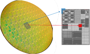 |
| 300mm Si wafer exposed on FLX-1200 multi-beam tool at 5kV on N40 BEOL stack |
Abstract:
Leti, a research institute of CEA Tech, and Mapper Lithography, the leading provider of maskless lithography equipment for the semiconductor and nanofabrication industries, today announced a low-cost cyber-security breakthrough that encrypts individual chips with a code.
Leti & Mapper announce cyber-security breakthrough that encrypts individual chips with a code: Low-Cost Cyber-Security Breakthrough that Encrypts Individual Chips With a Unique Code Presented at SPIE Advanced Lithography 2018 in San Jose
Grenoble, France and Delft, The Netherlands | Posted on March 2nd, 2018The non-falsifiable code is generated by using a unique chip design that leverages direct multi-beam writing in a process that fits in a conventional CMOS flow with an extra level of lithography and without photomasks. Throughput on Mapper�sFLX-1200 tool installed at Leti is compatible with optical systems.
The markets for these chips include data security, traceability and combatting imports of counterfeit chips.
Leti, a specialist in electron-beam lithography, and Mapper, a Dutch company, presented a paper on the breakthrough, �Process development of a maskless N40 via level for security application with multi-beam lithography�, today at SPIE Advanced Lithography 2018 in San Jose, Calif. The paper demonstrates a via patterning integration that is compliant with standard CMOS 40nm process flow.
�Standard optical exposure tools � optical scanners using masks � repeat the identical design on the entire silicon wafer, and cannot fabricate individualized chips,� said Leti�s Isabelle Servin, the lead author of the paper. �Leti applied its deep multi-beam lithography knowhow and Mapper�s unique maskless fabrication tools to achieve this differentiating, cyber-security chip.�
The maskless lithography system, based on massively parallel electron-beam writing capability developed by Mapper, is designed for high-volume specialty chips and low-volume advanced logic.
Leti and Mapper are demonstrating the breakthrough for their customers at Leti�s facility in Grenoble.
####
About Leti
Leti, a technology research institute at CEA Tech, is a global leader in miniaturization technologies enabling smart, energy-efficient and secure solutions for industry. Founded in 1967, Leti pioneers micro-& nanotechnologies, tailoring differentiating applicative solutions for global companies, SMEs and startups. Leti tackles critical challenges in healthcare, energy and digital migration. From sensors to data processing and computing solutions, Leti�s multidisciplinary teams deliver solid expertise, leveraging world-class pre-industrialization facilities. With a staff of more than 1,900, a portfolio of 2,700 patents, 91,500 sq. ft. of cleanroom space and a clear IP policy, the institute is based in Grenoble, France, and has offices in Silicon Valley and Tokyo. Leti has launched 60 startups and is a member of the Carnot Institutes network. Follow us on www.leti-cea.com and @CEA_Leti.
CEA Tech is the technology research branch of the French Alternative Energies and Atomic Energy Commission (CEA), a key player in innovative R&D, defence & security, nuclear energy, technological research for industry and fundamental science, identified by Thomson Reuters as the second most innovative research organization in the world. CEA Tech leverages a unique innovation-driven culture and unrivalled expertise to develop and disseminate new technologies for industry, helping to create high-end products and provide a competitive edge.
About Mapper
Mapper, based in Delft, The Netherlands, is developing a groundbreaking maskless lithography infrastructure for the semiconductor and nanofabrication industry. The capabilities of a maskless patterning system with 65,000 electron beams enable unique functionalities in high volume nanofabrication and specialized logic. Typical examples are security and identification chips and integrated optics functionalities on image sensors for smart phones. Mapper employs 270 people.
For further information, please visit mapper.nl
For more information, please click here
Contacts:
Press Contact
Agency
+33 6 74 93 23 47
Copyright © Leti
If you have a comment, please Contact us.Issuers of news releases, not 7th Wave, Inc. or Nanotechnology Now, are solely responsible for the accuracy of the content.
Bookmark:


| Related News Press |
News and information
![]() Quantum computer improves AI predictions April 17th, 2026
Quantum computer improves AI predictions April 17th, 2026
![]() Flexible sensor gains sensitivity under pressure April 17th, 2026
Flexible sensor gains sensitivity under pressure April 17th, 2026
![]() A reusable chip for particulate matter sensing April 17th, 2026
A reusable chip for particulate matter sensing April 17th, 2026
![]() Detecting vibrational quantum beating in the predissociation dynamics of SF6 using time-resolved photoelectron spectroscopy April 17th, 2026
Detecting vibrational quantum beating in the predissociation dynamics of SF6 using time-resolved photoelectron spectroscopy April 17th, 2026
Law enforcement/Anti-Counterfeiting/Security/Loss prevention
![]() Chainmail-like material could be the future of armor: First 2D mechanically interlocked polymer exhibits exceptional flexibility and strength January 17th, 2025
Chainmail-like material could be the future of armor: First 2D mechanically interlocked polymer exhibits exceptional flexibility and strength January 17th, 2025
![]() With VECSELs towards the quantum internet Fraunhofer: IAF achieves record output power with VECSEL for quantum frequency converters April 5th, 2024
With VECSELs towards the quantum internet Fraunhofer: IAF achieves record output power with VECSEL for quantum frequency converters April 5th, 2024
![]() Researchers� approach may protect quantum computers from attacks March 8th, 2024
Researchers� approach may protect quantum computers from attacks March 8th, 2024
![]() New chip ramps up AI computing efficiency August 19th, 2022
New chip ramps up AI computing efficiency August 19th, 2022
Hardware
![]() The present and future of computing get a boost from new research July 21st, 2023
The present and future of computing get a boost from new research July 21st, 2023
![]() A Carbon Nanotube Microprocessor Mature Enough to Say Hello: Three new breakthroughs make commercial nanotube processors possible March 2nd, 2020
A Carbon Nanotube Microprocessor Mature Enough to Say Hello: Three new breakthroughs make commercial nanotube processors possible March 2nd, 2020
![]() Powering the future: Smallest all-digital circuit opens doors to 5 nm next-gen semiconductor February 11th, 2020
Powering the future: Smallest all-digital circuit opens doors to 5 nm next-gen semiconductor February 11th, 2020
Chip Technology
![]() A reusable chip for particulate matter sensing April 17th, 2026
A reusable chip for particulate matter sensing April 17th, 2026
![]() Metasurfaces smooth light to boost magnetic sensing precision January 30th, 2026
Metasurfaces smooth light to boost magnetic sensing precision January 30th, 2026
Nanoelectronics
![]() Lab to industry: InSe wafer-scale breakthrough for future electronics August 8th, 2025
Lab to industry: InSe wafer-scale breakthrough for future electronics August 8th, 2025
![]() Interdisciplinary: Rice team tackles the future of semiconductors Multiferroics could be the key to ultralow-energy computing October 6th, 2023
Interdisciplinary: Rice team tackles the future of semiconductors Multiferroics could be the key to ultralow-energy computing October 6th, 2023
![]() Key element for a scalable quantum computer: Physicists from Forschungszentrum J�lich and RWTH Aachen University demonstrate electron transport on a quantum chip September 23rd, 2022
Key element for a scalable quantum computer: Physicists from Forschungszentrum J�lich and RWTH Aachen University demonstrate electron transport on a quantum chip September 23rd, 2022
![]() Reduced power consumption in semiconductor devices September 23rd, 2022
Reduced power consumption in semiconductor devices September 23rd, 2022
Discoveries
![]() Quantum computer improves AI predictions April 17th, 2026
Quantum computer improves AI predictions April 17th, 2026
![]() Flexible sensor gains sensitivity under pressure April 17th, 2026
Flexible sensor gains sensitivity under pressure April 17th, 2026
![]() A reusable chip for particulate matter sensing April 17th, 2026
A reusable chip for particulate matter sensing April 17th, 2026
![]() Detecting vibrational quantum beating in the predissociation dynamics of SF6 using time-resolved photoelectron spectroscopy April 17th, 2026
Detecting vibrational quantum beating in the predissociation dynamics of SF6 using time-resolved photoelectron spectroscopy April 17th, 2026
Announcements
![]() A fundamentally new therapeutic approach to cystic fibrosis: Nanobody repairs cellular defect April 17th, 2026
A fundamentally new therapeutic approach to cystic fibrosis: Nanobody repairs cellular defect April 17th, 2026
![]() UC Irvine physicists discover method to reverse �quantum scrambling� : The work addresses the problem of information loss in quantum computing system April 17th, 2026
UC Irvine physicists discover method to reverse �quantum scrambling� : The work addresses the problem of information loss in quantum computing system April 17th, 2026
Events/Classes
![]() Institute for Nanoscience hosts annual proposal planning meeting May 16th, 2025
Institute for Nanoscience hosts annual proposal planning meeting May 16th, 2025
![]() A New Blue: Mysterious origin of the ribbontail ray�s electric blue spots revealed July 5th, 2024
A New Blue: Mysterious origin of the ribbontail ray�s electric blue spots revealed July 5th, 2024
![]() Researchers demonstrate co-propagation of quantum and classical signals: Study shows that quantum encryption can be implemented in existing fiber networks January 20th, 2023
Researchers demonstrate co-propagation of quantum and classical signals: Study shows that quantum encryption can be implemented in existing fiber networks January 20th, 2023
Printing/Lithography/Inkjet/Inks/Bio-printing/Dyes
![]() Presenting: Ultrasound-based printing of 3D materials�potentially inside the body December 8th, 2023
Presenting: Ultrasound-based printing of 3D materials�potentially inside the body December 8th, 2023
![]() Simple ballpoint pen can write custom LEDs August 11th, 2023
Simple ballpoint pen can write custom LEDs August 11th, 2023
![]() Disposable electronics on a simple sheet of paper October 7th, 2022
Disposable electronics on a simple sheet of paper October 7th, 2022
|
|
||
|
|
||
| The latest news from around the world, FREE | ||
|
|
||
|
|
||
| Premium Products | ||
|
|
||
|
Only the news you want to read!
Learn More |
||
|
|
||
|
Full-service, expert consulting
Learn More |
||
|
|
||