Home > Press > Scientists reveal the fundamental limitation in the key material for solid-state lighting
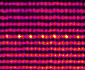 |
| This is a scanning transmission electron microscopy image of the atomic ordering in (In, Ga)N monolayer: single atomic column, containing only indium (In) atoms (shown by higher intensity on the image), followed by two, containing only gallium (Ga) atoms. CREDIT IKZ Berlin |
Abstract:
For the first time an international research group has revealed the core mechanism that limits the indium (In) content in indium gallium nitride ((In, Ga)N) thin films - the key material for blue light emitting diodes (LED). Increasing the In content in InGaN quantum wells is the common approach to shift the emission of III-Nitride based LEDs towards the green and, in particular, red part of the optical spectrum, necessary for the modern RGB devices. The new findings answer the long-standing research question: why does this classical approach fail, when we try to obtain efficient InGaN-based green and red LEDs?
Scientists reveal the fundamental limitation in the key material for solid-state lighting
Berlin, Germany | Posted on January 25th, 2018Despite the progress in the field of green LEDs and lasers, the researchers could not overcome the limit of 30% of indium content in the films. The reason for that was unclear up to now: is it a problem of finding the right growth conditions or rather a fundamental effect that cannot be overcome? Now, an international team from Germany, Poland and China has shed new light on this question and revealed the mechanism responsible for that limitation.
In their work the scientists tried to push the indium content to the limit by growing single atomic layers of InN on GaN. However, independent on growth conditions, indium concentrations have never exceeded 25% - 30% - a clear sign of a fundamentally limiting mechanism. The researchers used advanced characterization methods, such as atomic resolution transmission electron microscope (TEM) and in-situ reflection high-energy electron diffraction (RHEED), and discovered that, as soon as the indium content reaches around 25 %, the atoms within the (In, Ga)N monolayer arrange in a regular pattern - single atomic column of In alternates with two atomic columns of Ga atoms. Comprehensive theoretical calculations revealed that the atomic ordering is induced by a particular surface reconstruction: indium atoms are bonded with four neighboring atoms, instead of expected three. This creates stronger bonds between indium and nitrogen atoms, which, on one hand, allows to use higher temperatures during the growth and provides material with better quality. On the other hand, the ordering sets the limit of the In content of 25%, which cannot be overcome under realistic growth conditions.
"Apparently, a technological bottleneck hampers all the attempts to shift the emission from the green towards the yellow and the red regions of the spectra. Therefore, new original pathways are urgently required to overcome these fundamental limitations," states Dr. Tobias Schulz, scientist at the Leibniz-Institut fuer Kristallzuechtung; "for example, growth of InGaN films on high quality InGaN pseudo-substrates that would reduce the strain in the growing layer."
However, the discovery of ordering may help to overcome well known limitations of the InGaN material system: localization of charge carriers due to fluctuations in the chemical composition of the alloy. Growing stable ordered (In, Ga)N alloys with the fixed composition at high temperatures could thus improve the optical properties of devices.
###
The work is a result of a collaboration between Leibniz-Institut fuer Kristallzuechtung (Berlin, Germany), Max-Planck-Institut fuer Eisenforschung (Duesseldorf, Germany), Paul-Drude Institut fuer Festkoerperelektronik (Berlin, Germany), Institute of High-Pressure Physics (Warsaw, Poland), and State Key Laboratory of Artificial Microstructure and Mesoscopic Physics (Beijing, China).
####
For more information, please click here
Contacts:
Stefanie Grueber
49-306-392-3263
Copyright © Forschngsverbund Berlin
If you have a comment, please Contact us.Issuers of news releases, not 7th Wave, Inc. or Nanotechnology Now, are solely responsible for the accuracy of the content.
Bookmark:


| Related Links |
| Related News Press |
News and information
![]() Quantum computer improves AI predictions April 17th, 2026
Quantum computer improves AI predictions April 17th, 2026
![]() Flexible sensor gains sensitivity under pressure April 17th, 2026
Flexible sensor gains sensitivity under pressure April 17th, 2026
![]() A reusable chip for particulate matter sensing April 17th, 2026
A reusable chip for particulate matter sensing April 17th, 2026
![]() Detecting vibrational quantum beating in the predissociation dynamics of SF6 using time-resolved photoelectron spectroscopy April 17th, 2026
Detecting vibrational quantum beating in the predissociation dynamics of SF6 using time-resolved photoelectron spectroscopy April 17th, 2026
Thin films
![]() Tiny nanosheets, big leap: A new sensor detects ethanol at ultra-low levels January 30th, 2026
Tiny nanosheets, big leap: A new sensor detects ethanol at ultra-low levels January 30th, 2026
Display technology/LEDs/SS Lighting/OLEDs
![]() Spinel-type sulfide semiconductors to operate the next-generation LEDs and solar cells For solar-cell absorbers and green-LED source October 3rd, 2025
Spinel-type sulfide semiconductors to operate the next-generation LEDs and solar cells For solar-cell absorbers and green-LED source October 3rd, 2025
![]() Efficient and stable hybrid perovskite-organic light-emitting diodes with external quantum efficiency exceeding 40 per cent July 5th, 2024
Efficient and stable hybrid perovskite-organic light-emitting diodes with external quantum efficiency exceeding 40 per cent July 5th, 2024
Possible Futures
![]() A fundamentally new therapeutic approach to cystic fibrosis: Nanobody repairs cellular defect April 17th, 2026
A fundamentally new therapeutic approach to cystic fibrosis: Nanobody repairs cellular defect April 17th, 2026
![]() UC Irvine physicists discover method to reverse �quantum scrambling� : The work addresses the problem of information loss in quantum computing system April 17th, 2026
UC Irvine physicists discover method to reverse �quantum scrambling� : The work addresses the problem of information loss in quantum computing system April 17th, 2026
Discoveries
![]() Quantum computer improves AI predictions April 17th, 2026
Quantum computer improves AI predictions April 17th, 2026
![]() Flexible sensor gains sensitivity under pressure April 17th, 2026
Flexible sensor gains sensitivity under pressure April 17th, 2026
![]() A reusable chip for particulate matter sensing April 17th, 2026
A reusable chip for particulate matter sensing April 17th, 2026
![]() Detecting vibrational quantum beating in the predissociation dynamics of SF6 using time-resolved photoelectron spectroscopy April 17th, 2026
Detecting vibrational quantum beating in the predissociation dynamics of SF6 using time-resolved photoelectron spectroscopy April 17th, 2026
Materials/Metamaterials/Magnetoresistance
![]() First real-time observation of two-dimensional melting process: Researchers at Mainz University unveil new insights into magnetic vortex structures August 8th, 2025
First real-time observation of two-dimensional melting process: Researchers at Mainz University unveil new insights into magnetic vortex structures August 8th, 2025
![]() Researchers unveil a groundbreaking clay-based solution to capture carbon dioxide and combat climate change June 6th, 2025
Researchers unveil a groundbreaking clay-based solution to capture carbon dioxide and combat climate change June 6th, 2025
![]() A 1960s idea inspires NBI researchers to study hitherto inaccessible quantum states June 6th, 2025
A 1960s idea inspires NBI researchers to study hitherto inaccessible quantum states June 6th, 2025
![]() Institute for Nanoscience hosts annual proposal planning meeting May 16th, 2025
Institute for Nanoscience hosts annual proposal planning meeting May 16th, 2025
Announcements
![]() A fundamentally new therapeutic approach to cystic fibrosis: Nanobody repairs cellular defect April 17th, 2026
A fundamentally new therapeutic approach to cystic fibrosis: Nanobody repairs cellular defect April 17th, 2026
![]() UC Irvine physicists discover method to reverse �quantum scrambling� : The work addresses the problem of information loss in quantum computing system April 17th, 2026
UC Irvine physicists discover method to reverse �quantum scrambling� : The work addresses the problem of information loss in quantum computing system April 17th, 2026
Interviews/Book Reviews/Essays/Reports/Podcasts/Journals/White papers/Posters
![]() A fundamentally new therapeutic approach to cystic fibrosis: Nanobody repairs cellular defect April 17th, 2026
A fundamentally new therapeutic approach to cystic fibrosis: Nanobody repairs cellular defect April 17th, 2026
![]() UC Irvine physicists discover method to reverse �quantum scrambling� : The work addresses the problem of information loss in quantum computing system April 17th, 2026
UC Irvine physicists discover method to reverse �quantum scrambling� : The work addresses the problem of information loss in quantum computing system April 17th, 2026
Quantum nanoscience
![]() Beyond silicon: Electronics at the scale of a single molecule January 30th, 2026
Beyond silicon: Electronics at the scale of a single molecule January 30th, 2026
![]() MXene nanomaterials enter a new dimension Multilayer nanomaterial: MXene flakes created at Drexel University show new promise as 1D scrolls January 30th, 2026
MXene nanomaterials enter a new dimension Multilayer nanomaterial: MXene flakes created at Drexel University show new promise as 1D scrolls January 30th, 2026
![]() ICFO researchers overcome long-standing bottleneck in single photon detection with twisted 2D materials August 8th, 2025
ICFO researchers overcome long-standing bottleneck in single photon detection with twisted 2D materials August 8th, 2025
|
|
||
|
|
||
| The latest news from around the world, FREE | ||
|
|
||
|
|
||
| Premium Products | ||
|
|
||
|
Only the news you want to read!
Learn More |
||
|
|
||
|
Full-service, expert consulting
Learn More |
||
|
|
||