Home > Press > Thanks for the memory: NIST takes a deep look at memristors
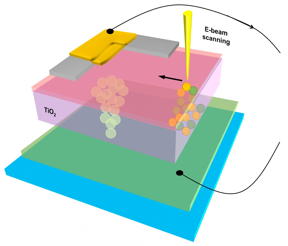 |
| Illustration shows an electron beam impinging on a section of a memristor, a device whose resistance depends on the memory of past current flow. As the beam strikes different parts of the memristor, it induces different currents, yielding a complete image of variations in the current throughout the device. Some of these variations in current indicate places where defects may occur, indicated by overlapping circles in the filament (titanium dioxide), where memory is stored. CREDIT NIST |
Abstract:
n the race to build a computer that mimics the massive computational power of the human brain, researchers are increasingly turning to memristors, which can vary their electrical resistance based on the memory of past activity. Scientists at the National Institute of Standards and Technology (NIST) have now unveiled the long-mysterious inner workings of these semiconductor elements, which can act like the short-term memory of nerve cells.
Thanks for the memory: NIST takes a deep look at memristors
Gaithersburg, MD | Posted on January 20th, 2018Just as the ability of one nerve cell to signal another depends on how often the cells have communicated in the recent past, the resistance of a memristor depends on the amount of current that recently flowed through it. Moreover, a memristor retains that memory even when electrical power is switched off.
But despite the keen interest in memristors, scientists have lacked a detailed understanding of how these devices work and have yet to develop a standard toolset to study them.
Now, NIST scientists have identified such a toolset and used it to more deeply probe how memristors operate. Their findings could lead to more efficient operation of the devices and suggest ways to minimize the leakage of current.
Brian Hoskins of NIST and the University of California, Santa Barbara, along with NIST scientists Nikolai Zhitenev, Andrei Kolmakov, Jabez McClelland and their colleagues from the University of Maryland's NanoCenter in College Park and the Institute for Research and Development in Microtechnologies in Bucharest, reported the findings in a recent Nature Communications.
To explore the electrical function of memristors, the team aimed a tightly focused beam of electrons at different locations on a titanium dioxide memristor. The beam knocked free some of the device's electrons, which formed ultrasharp images of those locations. The beam also induced four distinct currents to flow within the device. The team determined that the currents are associated with the multiple interfaces between materials in the memristor, which consists of two metal (conducting) layers separated by an insulator.
"We know exactly where each of the currents are coming from because we are controlling the location of the beam that is inducing those currents," said Hoskins.
In imaging the device, the team found several dark spots--regions of enhanced conductivity--which indicated places where current might leak out of the memristor during its normal operation. These leakage pathways resided outside the memristor's core--where it switches between the low and high resistance levels that are useful in an electronic device. The finding suggests that reducing the size of a memristor could minimize or even eliminate some of the unwanted current pathways. Although researchers had suspected that might be the case, they had lacked experimental guidance about just how much to reduce the size of the device.
Because the leakage pathways are tiny, involving distances of only 100 to 300 nanometers, "you're probably not going to start seeing some really big improvements until you reduce dimensions of the memristor on that scale," Hoskins said.
To their surprise, the team also found that the current that correlated with the memristor's switch in resistance didn't come from the active switching material at all, but the metal layer above it. The most important lesson of the memristor study, Hoskins noted, "is that you can't just worry about the resistive switch, the switching spot itself, you have to worry about everything around it." The team's study, he added, "is a way of generating much stronger intuition about what might be a good way to engineer memristors."
###
The NIST work was performed at the Center for Nanoscale Science and Technology (CNST), a shared-use facility available to researchers from industry, academia and government.
####
For more information, please click here
Contacts:
Ben P. Stein
301-975-2763
Copyright © NIST
If you have a comment, please Contact us.Issuers of news releases, not 7th Wave, Inc. or Nanotechnology Now, are solely responsible for the accuracy of the content.
Bookmark:


| Related Links |
| Related News Press |
News and information
![]() Quantum computer improves AI predictions April 17th, 2026
Quantum computer improves AI predictions April 17th, 2026
![]() Flexible sensor gains sensitivity under pressure April 17th, 2026
Flexible sensor gains sensitivity under pressure April 17th, 2026
![]() A reusable chip for particulate matter sensing April 17th, 2026
A reusable chip for particulate matter sensing April 17th, 2026
![]() Detecting vibrational quantum beating in the predissociation dynamics of SF6 using time-resolved photoelectron spectroscopy April 17th, 2026
Detecting vibrational quantum beating in the predissociation dynamics of SF6 using time-resolved photoelectron spectroscopy April 17th, 2026
Laboratories
![]() Researchers develop molecular qubits that communicate at telecom frequencies October 3rd, 2025
Researchers develop molecular qubits that communicate at telecom frequencies October 3rd, 2025
![]() A battery�s hopping ions remember where they�ve been: Seen in atomic detail, the seemingly smooth flow of ions through a battery�s electrolyte is surprisingly complicated February 16th, 2024
A battery�s hopping ions remember where they�ve been: Seen in atomic detail, the seemingly smooth flow of ions through a battery�s electrolyte is surprisingly complicated February 16th, 2024
Memristors
![]() Photoinduced large polaron transport and dynamics in organic-inorganic hybrid lead halide perovskite with terahertz probes July 8th, 2022
Photoinduced large polaron transport and dynamics in organic-inorganic hybrid lead halide perovskite with terahertz probes July 8th, 2022
![]() Artificial neurons go quantum with photonic circuits: Quantum memristor as missing link between artificial intelligence and quantum computing March 25th, 2022
Artificial neurons go quantum with photonic circuits: Quantum memristor as missing link between artificial intelligence and quantum computing March 25th, 2022
![]() New brain-like computing device simulates human learning: Researchers conditioned device to learn by association, like Pavlov's dog April 30th, 2021
New brain-like computing device simulates human learning: Researchers conditioned device to learn by association, like Pavlov's dog April 30th, 2021
Govt.-Legislation/Regulation/Funding/Policy
![]() Quantum computer improves AI predictions April 17th, 2026
Quantum computer improves AI predictions April 17th, 2026
![]() Metasurfaces smooth light to boost magnetic sensing precision January 30th, 2026
Metasurfaces smooth light to boost magnetic sensing precision January 30th, 2026
![]() New imaging approach transforms study of bacterial biofilms August 8th, 2025
New imaging approach transforms study of bacterial biofilms August 8th, 2025
Chip Technology
![]() A reusable chip for particulate matter sensing April 17th, 2026
A reusable chip for particulate matter sensing April 17th, 2026
![]() Metasurfaces smooth light to boost magnetic sensing precision January 30th, 2026
Metasurfaces smooth light to boost magnetic sensing precision January 30th, 2026
Memory Technology
![]() Researchers tackle the memory bottleneck stalling quantum computing October 3rd, 2025
Researchers tackle the memory bottleneck stalling quantum computing October 3rd, 2025
![]() First real-time observation of two-dimensional melting process: Researchers at Mainz University unveil new insights into magnetic vortex structures August 8th, 2025
First real-time observation of two-dimensional melting process: Researchers at Mainz University unveil new insights into magnetic vortex structures August 8th, 2025
![]() Utilizing palladium for addressing contact issues of buried oxide thin film transistors April 5th, 2024
Utilizing palladium for addressing contact issues of buried oxide thin film transistors April 5th, 2024
Discoveries
![]() Quantum computer improves AI predictions April 17th, 2026
Quantum computer improves AI predictions April 17th, 2026
![]() Flexible sensor gains sensitivity under pressure April 17th, 2026
Flexible sensor gains sensitivity under pressure April 17th, 2026
![]() A reusable chip for particulate matter sensing April 17th, 2026
A reusable chip for particulate matter sensing April 17th, 2026
![]() Detecting vibrational quantum beating in the predissociation dynamics of SF6 using time-resolved photoelectron spectroscopy April 17th, 2026
Detecting vibrational quantum beating in the predissociation dynamics of SF6 using time-resolved photoelectron spectroscopy April 17th, 2026
Announcements
![]() A fundamentally new therapeutic approach to cystic fibrosis: Nanobody repairs cellular defect April 17th, 2026
A fundamentally new therapeutic approach to cystic fibrosis: Nanobody repairs cellular defect April 17th, 2026
![]() UC Irvine physicists discover method to reverse �quantum scrambling� : The work addresses the problem of information loss in quantum computing system April 17th, 2026
UC Irvine physicists discover method to reverse �quantum scrambling� : The work addresses the problem of information loss in quantum computing system April 17th, 2026
Interviews/Book Reviews/Essays/Reports/Podcasts/Journals/White papers/Posters
![]() A fundamentally new therapeutic approach to cystic fibrosis: Nanobody repairs cellular defect April 17th, 2026
A fundamentally new therapeutic approach to cystic fibrosis: Nanobody repairs cellular defect April 17th, 2026
![]() UC Irvine physicists discover method to reverse �quantum scrambling� : The work addresses the problem of information loss in quantum computing system April 17th, 2026
UC Irvine physicists discover method to reverse �quantum scrambling� : The work addresses the problem of information loss in quantum computing system April 17th, 2026
|
|
||
|
|
||
| The latest news from around the world, FREE | ||
|
|
||
|
|
||
| Premium Products | ||
|
|
||
|
Only the news you want to read!
Learn More |
||
|
|
||
|
Full-service, expert consulting
Learn More |
||
|
|
||