Home > Press > A transistor of graphene nanoribbons: Breakthrough in Nanoelectronics
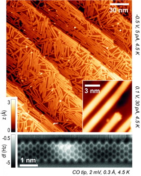 |
| The microscopic ribbons lie criss-crossed on the gold substrate. CREDIT EMPA |
Abstract:
Graphene ribbons that are only a few atoms wide, so-called graphene nanoribbons, have special electrical properties that make them promising candidates for the nanoelectronics of the future: While graphene - a one atom thin, honeycomb-shaped carbon layer - is a conductive material, it can become a semiconductor in the form of nanoribbons. This means that it has a sufficiently large energy or band gap in which no electron states can exist: it can be turned on and off - and thus may become a key component of nanotransistors.
A transistor of graphene nanoribbons: Breakthrough in Nanoelectronics
St. Gallen, Switzerland | Posted on November 29th, 2017The smallest details in the atomic structure of these graphene bands, however, have massive effects on the size of the energy gap and thus on how well-suited nanoribbons are as components of transistors. On the one hand, the gap depends on the width of the graphene ribbons, while on the other hand it depends on the structure of the edges. Since graphene consists of equilateral carbon hexagons, the border may have a zigzag or a so-called armchair shape, depending on the orientation of the ribbons. While bands with a zigzag edge behave like metals, i.e. they are conductive, they become semiconductors with the armchair edge.
This poses a major challenge for the production of nanoribbons: If the ribbons are cut from a layer of graphene or made by cutting carbon nanotubes, the edges may be irregular and thus the graphene ribbons may not exhibit the desired electrical properties.
Creating a semiconductor with nine atoms
Empa researchers in collaboration with the Max Planck Institute for Polymer Research in Mainz and the University of California at Berkeley have now succeeded in growing ribbons exactly nine atoms wide with a regular armchair edge from precursor molecules. The specially prepared molecules are evaporated in an ultra-high vacuum for this purpose. After several process steps, they are combined like puzzle pieces on a gold base to form the desired nanoribbons of about one nanometer in width and up to 50 nanometers in length.
These structures, which can only be seen with a scanning tunneling microscope, now have a relatively large and, above all, precisely defined energy gap. This enabled the researchers to go one step further and integrate the graphene ribbons into nanotransistors. Initially, however, the first attempts were not very successful: Measurements showed that the difference in the current flow between the "ON" state (i.e. with applied voltage) and the "OFF" state (without applied voltage) was far too small. The problem was the dielectric layer of silicon oxide, which connects the semiconducting layers to the electrical switch contact. In order to have the desired properties, it needed to be 50 nanometers thick, which in turn influenced the behavior of the electrons.
However, the researchers subsequently succeeded in massively reducing this layer by using hafnium oxide(HfO2) instead of silicon oxide as the dielectric material. The layer is therefore now only 1.5 nanometers thin and the "on"-current is orders of magnitudes higher.
Another problem was the incorporation of graphene ribbons into the transistor. In the future, the ribbons should no longer be located criss-cross on the transistor substrate, but rather aligned exactly along the transistor channel. This would significantly reduce the currently high level of non-functioning nanotransistors.
####
For more information, please click here
Contacts:
Dr. Gabriela Borin Barin
41-587-656-123
Copyright © EMPA
If you have a comment, please Contact us.Issuers of news releases, not 7th Wave, Inc. or Nanotechnology Now, are solely responsible for the accuracy of the content.
Bookmark:


| Related Links |
| Related News Press |
News and information
![]() Quantum computer improves AI predictions April 17th, 2026
Quantum computer improves AI predictions April 17th, 2026
![]() Flexible sensor gains sensitivity under pressure April 17th, 2026
Flexible sensor gains sensitivity under pressure April 17th, 2026
![]() A reusable chip for particulate matter sensing April 17th, 2026
A reusable chip for particulate matter sensing April 17th, 2026
![]() Detecting vibrational quantum beating in the predissociation dynamics of SF6 using time-resolved photoelectron spectroscopy April 17th, 2026
Detecting vibrational quantum beating in the predissociation dynamics of SF6 using time-resolved photoelectron spectroscopy April 17th, 2026
Graphene/ Graphite
![]() Electrifying results shed light on graphene foam as a potential material for lab grown cartilage June 6th, 2025
Electrifying results shed light on graphene foam as a potential material for lab grown cartilage June 6th, 2025
![]() Breakthrough in proton barrier films using pore-free graphene oxide: Kumamoto University researchers achieve new milestone in advanced coating technologies September 13th, 2024
Breakthrough in proton barrier films using pore-free graphene oxide: Kumamoto University researchers achieve new milestone in advanced coating technologies September 13th, 2024
Chip Technology
![]() A reusable chip for particulate matter sensing April 17th, 2026
A reusable chip for particulate matter sensing April 17th, 2026
![]() Metasurfaces smooth light to boost magnetic sensing precision January 30th, 2026
Metasurfaces smooth light to boost magnetic sensing precision January 30th, 2026
Discoveries
![]() Quantum computer improves AI predictions April 17th, 2026
Quantum computer improves AI predictions April 17th, 2026
![]() Flexible sensor gains sensitivity under pressure April 17th, 2026
Flexible sensor gains sensitivity under pressure April 17th, 2026
![]() A reusable chip for particulate matter sensing April 17th, 2026
A reusable chip for particulate matter sensing April 17th, 2026
![]() Detecting vibrational quantum beating in the predissociation dynamics of SF6 using time-resolved photoelectron spectroscopy April 17th, 2026
Detecting vibrational quantum beating in the predissociation dynamics of SF6 using time-resolved photoelectron spectroscopy April 17th, 2026
Materials/Metamaterials/Magnetoresistance
![]() First real-time observation of two-dimensional melting process: Researchers at Mainz University unveil new insights into magnetic vortex structures August 8th, 2025
First real-time observation of two-dimensional melting process: Researchers at Mainz University unveil new insights into magnetic vortex structures August 8th, 2025
![]() Researchers unveil a groundbreaking clay-based solution to capture carbon dioxide and combat climate change June 6th, 2025
Researchers unveil a groundbreaking clay-based solution to capture carbon dioxide and combat climate change June 6th, 2025
![]() A 1960s idea inspires NBI researchers to study hitherto inaccessible quantum states June 6th, 2025
A 1960s idea inspires NBI researchers to study hitherto inaccessible quantum states June 6th, 2025
![]() Institute for Nanoscience hosts annual proposal planning meeting May 16th, 2025
Institute for Nanoscience hosts annual proposal planning meeting May 16th, 2025
Announcements
![]() A fundamentally new therapeutic approach to cystic fibrosis: Nanobody repairs cellular defect April 17th, 2026
A fundamentally new therapeutic approach to cystic fibrosis: Nanobody repairs cellular defect April 17th, 2026
![]() UC Irvine physicists discover method to reverse �quantum scrambling� : The work addresses the problem of information loss in quantum computing system April 17th, 2026
UC Irvine physicists discover method to reverse �quantum scrambling� : The work addresses the problem of information loss in quantum computing system April 17th, 2026
Interviews/Book Reviews/Essays/Reports/Podcasts/Journals/White papers/Posters
![]() A fundamentally new therapeutic approach to cystic fibrosis: Nanobody repairs cellular defect April 17th, 2026
A fundamentally new therapeutic approach to cystic fibrosis: Nanobody repairs cellular defect April 17th, 2026
![]() UC Irvine physicists discover method to reverse �quantum scrambling� : The work addresses the problem of information loss in quantum computing system April 17th, 2026
UC Irvine physicists discover method to reverse �quantum scrambling� : The work addresses the problem of information loss in quantum computing system April 17th, 2026
|
|
||
|
|
||
| The latest news from around the world, FREE | ||
|
|
||
|
|
||
| Premium Products | ||
|
|
||
|
Only the news you want to read!
Learn More |
||
|
|
||
|
Full-service, expert consulting
Learn More |
||
|
|
||