Home > Press > Seeing the next dimension of computer chips: Researchers image perfectly smooth side-surfaces of 3-D silicon crystals with a scanning tunneling microscope, paving the way for smaller and faster computing devices
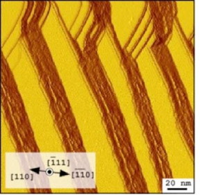 |
| Spatial-derivative STM images with 200x200 nm^2 at Vs = +1.5 V. Flat terraces become brighter and edges darker. The downstairs direction runs from left ((110) top-surface) to right ((-1-10) back-surface). CREDIT Osaka University |
Abstract:
A research collaboration between Osaka University and the Nara Institute of Science and Technology for the first time used scanning tunneling microscopy (STM) to create images of atomically flat side-surfaces of 3D silicon crystals. This work helps semiconductor manufacturers continue to innovate while producing smaller, faster, and more energy-efficient computer chips for computers and smartphones.
Seeing the next dimension of computer chips: Researchers image perfectly smooth side-surfaces of 3-D silicon crystals with a scanning tunneling microscope, paving the way for smaller and faster computing devices
Osaka, Japan | Posted on October 11th, 2017Our computers and smartphones each are loaded with millions of tiny transistors. The processing speed of these devices has increased dramatically over time as the number of transistors that can fit on a single computer chip continues to increase. Based on Moore's Law, the number of transistors per chip will double about every 2 years, and in this area it seems to be holding up. To keep up this pace of rapid innovation, computer manufacturers are continually on the lookout for new methods to make each transistor ever smaller.
Current microprocessors are made by adding patterns of circuits to flat silicon wafers. A novel way to cram more transistors in the same space is to fabricate 3D-structures. Fin-type field effect transistors (FETs) are named as such because they have fin-like silicon structures that extend into the air, off the surface of the chip. However, this new method requires a silicon crystal with a perfectly flat top and side-surfaces, instead of just the top surface, as with current devices. Designing the next generation of chips will require new knowledge of the atomic structures of the side-surfaces.
Now, researchers at Osaka University and the Nara Institute of Science and Technology report that they have used STM to image the side-surface of a silicon crystal for the first time. STM is a powerful technique that allows the locations of the individual silicon atoms to be seen. By passing a sharp tip very close to the sample, electrons can jump across the gap and create an electrical current. The microscope monitored this current, and determined the location of the atoms in the sample.
"Our study is a big first step toward the atomically resolved evaluation of transistors designed to have 3D-shapes," study coauthor Azusa Hattori says.
To make the side-surfaces as smooth as possible, the researchers first treated the crystals with a process called reactive ion etching. Coauthor Hidekazu Tanaka says, "Our ability to directly look at the side-surfaces using STM proves that we can make artificial 3D structures with near-perfect atomic surface ordering."
####
For more information, please click here
Contacts:
Saori Obayashi
81-661-055-886
Copyright © Osaka University
If you have a comment, please Contact us.Issuers of news releases, not 7th Wave, Inc. or Nanotechnology Now, are solely responsible for the accuracy of the content.
Bookmark:


| Related Links |
| Related News Press |
News and information
![]() Quantum computer improves AI predictions April 17th, 2026
Quantum computer improves AI predictions April 17th, 2026
![]() Flexible sensor gains sensitivity under pressure April 17th, 2026
Flexible sensor gains sensitivity under pressure April 17th, 2026
![]() A reusable chip for particulate matter sensing April 17th, 2026
A reusable chip for particulate matter sensing April 17th, 2026
![]() Detecting vibrational quantum beating in the predissociation dynamics of SF6 using time-resolved photoelectron spectroscopy April 17th, 2026
Detecting vibrational quantum beating in the predissociation dynamics of SF6 using time-resolved photoelectron spectroscopy April 17th, 2026
Imaging
![]() Simple algorithm paired with standard imaging tool could predict failure in lithium metal batteries August 8th, 2025
Simple algorithm paired with standard imaging tool could predict failure in lithium metal batteries August 8th, 2025
Possible Futures
![]() A fundamentally new therapeutic approach to cystic fibrosis: Nanobody repairs cellular defect April 17th, 2026
A fundamentally new therapeutic approach to cystic fibrosis: Nanobody repairs cellular defect April 17th, 2026
![]() UC Irvine physicists discover method to reverse �quantum scrambling� : The work addresses the problem of information loss in quantum computing system April 17th, 2026
UC Irvine physicists discover method to reverse �quantum scrambling� : The work addresses the problem of information loss in quantum computing system April 17th, 2026
Chip Technology
![]() A reusable chip for particulate matter sensing April 17th, 2026
A reusable chip for particulate matter sensing April 17th, 2026
![]() Metasurfaces smooth light to boost magnetic sensing precision January 30th, 2026
Metasurfaces smooth light to boost magnetic sensing precision January 30th, 2026
Nanoelectronics
![]() Lab to industry: InSe wafer-scale breakthrough for future electronics August 8th, 2025
Lab to industry: InSe wafer-scale breakthrough for future electronics August 8th, 2025
![]() Interdisciplinary: Rice team tackles the future of semiconductors Multiferroics could be the key to ultralow-energy computing October 6th, 2023
Interdisciplinary: Rice team tackles the future of semiconductors Multiferroics could be the key to ultralow-energy computing October 6th, 2023
![]() Key element for a scalable quantum computer: Physicists from Forschungszentrum J�lich and RWTH Aachen University demonstrate electron transport on a quantum chip September 23rd, 2022
Key element for a scalable quantum computer: Physicists from Forschungszentrum J�lich and RWTH Aachen University demonstrate electron transport on a quantum chip September 23rd, 2022
![]() Reduced power consumption in semiconductor devices September 23rd, 2022
Reduced power consumption in semiconductor devices September 23rd, 2022
Discoveries
![]() Quantum computer improves AI predictions April 17th, 2026
Quantum computer improves AI predictions April 17th, 2026
![]() Flexible sensor gains sensitivity under pressure April 17th, 2026
Flexible sensor gains sensitivity under pressure April 17th, 2026
![]() A reusable chip for particulate matter sensing April 17th, 2026
A reusable chip for particulate matter sensing April 17th, 2026
![]() Detecting vibrational quantum beating in the predissociation dynamics of SF6 using time-resolved photoelectron spectroscopy April 17th, 2026
Detecting vibrational quantum beating in the predissociation dynamics of SF6 using time-resolved photoelectron spectroscopy April 17th, 2026
Announcements
![]() A fundamentally new therapeutic approach to cystic fibrosis: Nanobody repairs cellular defect April 17th, 2026
A fundamentally new therapeutic approach to cystic fibrosis: Nanobody repairs cellular defect April 17th, 2026
![]() UC Irvine physicists discover method to reverse �quantum scrambling� : The work addresses the problem of information loss in quantum computing system April 17th, 2026
UC Irvine physicists discover method to reverse �quantum scrambling� : The work addresses the problem of information loss in quantum computing system April 17th, 2026
Interviews/Book Reviews/Essays/Reports/Podcasts/Journals/White papers/Posters
![]() A fundamentally new therapeutic approach to cystic fibrosis: Nanobody repairs cellular defect April 17th, 2026
A fundamentally new therapeutic approach to cystic fibrosis: Nanobody repairs cellular defect April 17th, 2026
![]() UC Irvine physicists discover method to reverse �quantum scrambling� : The work addresses the problem of information loss in quantum computing system April 17th, 2026
UC Irvine physicists discover method to reverse �quantum scrambling� : The work addresses the problem of information loss in quantum computing system April 17th, 2026
Tools
![]() Metasurfaces smooth light to boost magnetic sensing precision January 30th, 2026
Metasurfaces smooth light to boost magnetic sensing precision January 30th, 2026
![]() From sensors to smart systems: the rise of AI-driven photonic noses January 30th, 2026
From sensors to smart systems: the rise of AI-driven photonic noses January 30th, 2026
![]() Japan launches fully domestically produced quantum computer: Expo visitors to experience quantum computing firsthand August 8th, 2025
Japan launches fully domestically produced quantum computer: Expo visitors to experience quantum computing firsthand August 8th, 2025
Research partnerships
![]() Lab to industry: InSe wafer-scale breakthrough for future electronics August 8th, 2025
Lab to industry: InSe wafer-scale breakthrough for future electronics August 8th, 2025
![]() HKU physicists uncover hidden order in the quantum world through deconfined quantum critical points April 25th, 2025
HKU physicists uncover hidden order in the quantum world through deconfined quantum critical points April 25th, 2025
|
|
||
|
|
||
| The latest news from around the world, FREE | ||
|
|
||
|
|
||
| Premium Products | ||
|
|
||
|
Only the news you want to read!
Learn More |
||
|
|
||
|
Full-service, expert consulting
Learn More |
||
|
|
||