Home > Press > New method for analyzing crystal structure: Exotic materials called photonic crystals reveal their internal characteristics with new method
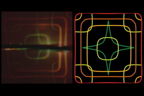 |
| This image shows theoretical (right) and experimental (left) iso-frequency contours of a photonic crystal slabs superimposed on each other. |
Abstract:
A new technique developed by MIT researchers reveals the inner details of photonic crystals, synthetic materials whose exotic optical properties are the subject of widespread research.
New method for analyzing crystal structure: Exotic materials called photonic crystals reveal their internal characteristics with new method
Cambridge, MA | Posted on November 30th, 2016Photonic crystals are generally made by drilling millions of closely spaced, minuscule holes in a slab of transparent material, using variations of microchip-fabrication methods. Depending on the exact orientation, size, and spacing of these holes, these materials can exhibit a variety of peculiar optical properties, including �superlensing,� which allows for magnification that pushes beyond the normal theoretical limits, and �negative refraction,� in which light is bent in a direction opposite to its path through normal transparent materials.
But to understand exactly how light of various colors and from various directions moves through photonic crystals requires extremely complex calculations. Researchers often use highly simplified approaches; for example they may only calculate the behavior of light along a single direction or for a single color.
Instead, the new technique makes the full range of information directly visible. Researchers can use a straightforward laboratory setup to display the information � a pattern of so-called �iso-frequency contours� � in a graphical form that can be simply photographed and examined, in many cases eliminating the need for calculations. The method is described this week in the journal Science Advances, in a paper by MIT postdoc Bo Zhen, recent Wellesley College graduate and MIT affiliate Emma Regan, MIT professors of physics Marin Soljačić and John Joannopoulos, and four others.
The discovery of this new technique, Zhen explains, came about by looking closely at a phenomenon that the researchers had noticed and even made use of for years, but whose origins they hadn�t previously understood. Patterns of scattered light seemed to fan out from samples of photonic materials when the samples were illuminated by laser light. The scattering was surprising, since the underlying crystalline structure was fabricated to be almost perfect in these materials.
�When we would try to do a lasing measurement, we would always see this pattern,� Zhen says. �We saw this shape, but we didn�t know what was happening.� But it did help them to get their experimental setup properly aligned, because the scattered light pattern would appear as soon as the laser beam was properly lined up with the crystal. Upon careful analysis, they realized the scattering patterns were generated by tiny defects in the crystal � holes that were not perfectly round in shape or that were slightly tapered from one end to the other.
�There is fabrication disorder even in the best samples that can be made,� Regan says. �People think that the scattering would be very weak, because the sample is nearly perfect,� but it turns out that at certain angles and frequencies, the light scatters very strongly; as much as 50 percent of the incoming light can be scattered. By illuminating the sample in turn with a sequence of different colors, it is possible to build up a full display of the relative paths light beams take, all across the visible spectrum. The scattered light produces a direct view of the iso-frequency contours � a sort of topographic map of the way light beams of different colors bend as they pass through the photonic crystal.
�This is a very beautiful, very direct way to observe the iso-frequency contours,� Soljačić says. �You just shine light at the sample, with the right direction and frequency,� and what comes out is a direct image of the needed information, he says.
The finding could potentially be useful for a number of different applications, the team says. For example, it could lead to a way of making large, transparent display screens, where most light would pass straight through as if through a window, but light of specific frequencies would be scattered to produce a clear image on the screen. Or, the method could be used to make private displays that would only be visible to the person directly in front of the screen.
Because it relies on imperfections in the fabrication of the crystal, this method could also be used as a quality-control measure for manufacturing of such materials; the images provide an indication of not only the total amount of imperfections, but also their specific nature � that is, whether the dominant disorder in the sample comes from noncircular holes or etches that aren�t straight � so that the process can be tuned and improved.
�Using a clever trick, the Soljačić group turned what is ordinarily a nuisance (i.e., unavoidable disorder in nanofabrication) to their advantage,� says Mikael Rechtsman, an assistant professor of physics at Pennsylvania State University who was not involved in this work. �The random scattering caused by the disorder allowed them to directly image the iso-frequency contours of the photonic crystal slab structure. Since any nanofabricated structure always has some degree of disorder, and since disorder is invariably difficult to model a priori in simulations, their method provides an extremely convenient characterization tool for photonic crystal resonant mode band structures.�
Rechtsman adds, �This could become an essential tool in the hunt for high-power single-mode semiconductor lasers (in particular, photonic crystal surface emitting lasers), with wide-ranging applications including telecommunications and manufacturing.�
The team also included researchers at MIT Research Laboratory of Electronics, including Yuichi Igarashi (now at NEC Corporation in Japan), Ido Kaminer, Chia Wei Hsu (now at Yale University), and Yichen Shen. The work was supported by the Army Research Office through the Institute for Soldier Nanotechnologies at MIT, and by the U.S. Department of Energy through S3TEC, an Energy Frontier Center.
####
For more information, please click here
Contacts:
Karl-Lydie Jean-Baptiste
Email:
Phone: (617) 253-1682
MIT News
Copyright © Massachusetts Institute of Technology
If you have a comment, please Contact us.Issuers of news releases, not 7th Wave, Inc. or Nanotechnology Now, are solely responsible for the accuracy of the content.
Bookmark:


| Related Links |
![]() Paper: "Direct imaging of isofrequency contours in photonic structures":
Paper: "Direct imaging of isofrequency contours in photonic structures":
| Related News Press |
News and information
![]() Quantum computer improves AI predictions April 17th, 2026
Quantum computer improves AI predictions April 17th, 2026
![]() Flexible sensor gains sensitivity under pressure April 17th, 2026
Flexible sensor gains sensitivity under pressure April 17th, 2026
![]() A reusable chip for particulate matter sensing April 17th, 2026
A reusable chip for particulate matter sensing April 17th, 2026
![]() Detecting vibrational quantum beating in the predissociation dynamics of SF6 using time-resolved photoelectron spectroscopy April 17th, 2026
Detecting vibrational quantum beating in the predissociation dynamics of SF6 using time-resolved photoelectron spectroscopy April 17th, 2026
Wireless/telecommunications/RF/Antennas/Microwaves
![]() Researchers develop molecular qubits that communicate at telecom frequencies October 3rd, 2025
Researchers develop molecular qubits that communicate at telecom frequencies October 3rd, 2025
![]() HKUST researchers develop new integration technique for efficient coupling of III-V and silicon February 16th, 2024
HKUST researchers develop new integration technique for efficient coupling of III-V and silicon February 16th, 2024
Govt.-Legislation/Regulation/Funding/Policy
![]() Quantum computer improves AI predictions April 17th, 2026
Quantum computer improves AI predictions April 17th, 2026
![]() Metasurfaces smooth light to boost magnetic sensing precision January 30th, 2026
Metasurfaces smooth light to boost magnetic sensing precision January 30th, 2026
![]() New imaging approach transforms study of bacterial biofilms August 8th, 2025
New imaging approach transforms study of bacterial biofilms August 8th, 2025
Possible Futures
![]() A fundamentally new therapeutic approach to cystic fibrosis: Nanobody repairs cellular defect April 17th, 2026
A fundamentally new therapeutic approach to cystic fibrosis: Nanobody repairs cellular defect April 17th, 2026
![]() UC Irvine physicists discover method to reverse �quantum scrambling� : The work addresses the problem of information loss in quantum computing system April 17th, 2026
UC Irvine physicists discover method to reverse �quantum scrambling� : The work addresses the problem of information loss in quantum computing system April 17th, 2026
Optical computing/Photonic computing
![]() ICFO researchers overcome long-standing bottleneck in single photon detection with twisted 2D materials August 8th, 2025
ICFO researchers overcome long-standing bottleneck in single photon detection with twisted 2D materials August 8th, 2025
![]() Programmable electron-induced color router array May 14th, 2025
Programmable electron-induced color router array May 14th, 2025
Discoveries
![]() Quantum computer improves AI predictions April 17th, 2026
Quantum computer improves AI predictions April 17th, 2026
![]() Flexible sensor gains sensitivity under pressure April 17th, 2026
Flexible sensor gains sensitivity under pressure April 17th, 2026
![]() A reusable chip for particulate matter sensing April 17th, 2026
A reusable chip for particulate matter sensing April 17th, 2026
![]() Detecting vibrational quantum beating in the predissociation dynamics of SF6 using time-resolved photoelectron spectroscopy April 17th, 2026
Detecting vibrational quantum beating in the predissociation dynamics of SF6 using time-resolved photoelectron spectroscopy April 17th, 2026
Announcements
![]() A fundamentally new therapeutic approach to cystic fibrosis: Nanobody repairs cellular defect April 17th, 2026
A fundamentally new therapeutic approach to cystic fibrosis: Nanobody repairs cellular defect April 17th, 2026
![]() UC Irvine physicists discover method to reverse �quantum scrambling� : The work addresses the problem of information loss in quantum computing system April 17th, 2026
UC Irvine physicists discover method to reverse �quantum scrambling� : The work addresses the problem of information loss in quantum computing system April 17th, 2026
Interviews/Book Reviews/Essays/Reports/Podcasts/Journals/White papers/Posters
![]() A fundamentally new therapeutic approach to cystic fibrosis: Nanobody repairs cellular defect April 17th, 2026
A fundamentally new therapeutic approach to cystic fibrosis: Nanobody repairs cellular defect April 17th, 2026
![]() UC Irvine physicists discover method to reverse �quantum scrambling� : The work addresses the problem of information loss in quantum computing system April 17th, 2026
UC Irvine physicists discover method to reverse �quantum scrambling� : The work addresses the problem of information loss in quantum computing system April 17th, 2026
Military
![]() Quantum engineers �squeeze� laser frequency combs to make more sensitive gas sensors January 17th, 2025
Quantum engineers �squeeze� laser frequency combs to make more sensitive gas sensors January 17th, 2025
![]() Chainmail-like material could be the future of armor: First 2D mechanically interlocked polymer exhibits exceptional flexibility and strength January 17th, 2025
Chainmail-like material could be the future of armor: First 2D mechanically interlocked polymer exhibits exceptional flexibility and strength January 17th, 2025
![]() Single atoms show their true color July 5th, 2024
Single atoms show their true color July 5th, 2024
![]() NRL charters Navy�s quantum inertial navigation path to reduce drift April 5th, 2024
NRL charters Navy�s quantum inertial navigation path to reduce drift April 5th, 2024
Photonics/Optics/Lasers
![]() Metasurfaces smooth light to boost magnetic sensing precision January 30th, 2026
Metasurfaces smooth light to boost magnetic sensing precision January 30th, 2026
![]() From sensors to smart systems: the rise of AI-driven photonic noses January 30th, 2026
From sensors to smart systems: the rise of AI-driven photonic noses January 30th, 2026
|
|
||
|
|
||
| The latest news from around the world, FREE | ||
|
|
||
|
|
||
| Premium Products | ||
|
|
||
|
Only the news you want to read!
Learn More |
||
|
|
||
|
Full-service, expert consulting
Learn More |
||
|
|
||