Home > Press > Novel silicon etching technique crafts 3-D gradient refractive index micro-optics
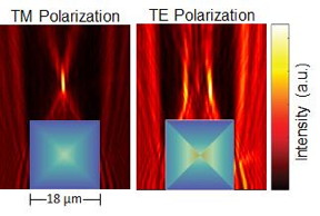 |
| Figure shows how the PSi square GRIN microlens focuses and splits TM and TE polarized light, respectively. TM polarized light is focused to one point and TE polarized light is focused to two different points. The refractive index gradient for the square microlens under the two different polarizations is illustrated using the color map overlaid on the lens (blue is low refractive index, and orange is high refractive index). CREDIT University of Illinois |
Abstract:
A multi-institutional research collaboration has created a novel approach for fabricating three-dimensional micro-optics through the shape-defined formation of porous silicon (PSi), with broad impacts in integrated optoelectronics, imaging, and photovoltaics.
Novel silicon etching technique crafts 3-D gradient refractive index micro-optics
Urbana, IL | Posted on November 28th, 2016Working with colleagues at Stanford and The Dow Chemical Company, researchers at the University of Illinois at Urbana-Champaign fabricated 3-D birefringent gradient refractive index (GRIN) micro-optics by electrochemically etching preformed Si micro-structures, like square columns, PSi structures with defined refractive index profiles.
"The emergence and growth of transformation optics over the past decade has revitalized interest in using GRIN optics to control light propagation," explained Paul Braun, the Ivan Racheff Professor of Materials Science and Engineering at Illinois. "In this work, we have figured out how to couple the starting shape of the silicon micro-structure and the etch conditions to realize a unique set of desirable optical qualities. For example, these elements exhibit novel polarization-dependent optical functions, including splitting and focusing, expanding the use of porous silicon for a wide range of integrated photonics applications.
"The key is that the optical properties are a function of the etch current," Braun said. "If you change the etch current, you change the refractive index. We also think that the fact that we can create the structures in silicon is important, as silicon is important for photovoltaic, imaging, and integrated optics applications.
"Our demonstration using a three-dimensional, lithographically-defined silicon platform not only displayed the power of GRIN optics, but it also illustrated it in a promising form factor and material for integration within photonic integrated circuits," stated Neil Krueger, a former PhD student in Braun's research group and first author of the paper, "Porous Silicon Gradient Refractive Index Micro-Optics," appearing in Nano Letters.
"The real novelty of our work is that we are doing this in a three-dimensional optical element," added Krueger, who has recently joined Honeywell Aerospace as a Scientist in Advanced Technology. "This gives added control over the behavior of our structures given that light follows curvilinear optical paths in optically inhomogeneous media such as GRIN elements. The birefringent nature of these structures is an added bonus because coupled birefringent/GRIN effects provide an opportunity for a GRIN element to perform distinct, polarization-selective operations."
According to the researchers, PSi was initially studied due to its visible luminescence at room temperature, but more recently, as this and other reports have shown, has proven to be a versatile optical material, as its nanoscale porosity (and thus refractive index) can be modulated during its electrochemical fabrication.
"The beauty of this 3D fabrication process is that it is fast and scalable," commented Weijun Zhou at Dow. "Large scale, nanostructured GRIN components can be readily made to enable a variety of new industry applications such as advanced imaging, microscopy, and beam shaping."
"Because the etching process enables modulation of the refractive index, this approach makes it possible to decouple the optical performance and the physical shape of the optical element," Braun added. "Thus, for example, a lens can be formed without having to conform to the shape that we think of for a lens, opening up new opportunities in the design of integrated silicon optics."
###
Paul Braun is also the director of the Frederick Seitz Materials Research Laboratory at Illinois. In addition to Braun, Krueger, and Zhou, co-authors of the paper include Seung-Kyun Kang, Christian R. Ocier, Glennys Mensing, and John A. Rogers (University of Illinois), Aaron L. Holsteen and Mark L. Brongersma (Stanford University).
####
For more information, please click here
Contacts:
Paul Braun
217-244-7293
Copyright © University of Illinois College of Engineering
If you have a comment, please Contact us.Issuers of news releases, not 7th Wave, Inc. or Nanotechnology Now, are solely responsible for the accuracy of the content.
Bookmark:


| Related Links |
| Related News Press |
News and information
![]() Quantum computer improves AI predictions April 17th, 2026
Quantum computer improves AI predictions April 17th, 2026
![]() Flexible sensor gains sensitivity under pressure April 17th, 2026
Flexible sensor gains sensitivity under pressure April 17th, 2026
![]() A reusable chip for particulate matter sensing April 17th, 2026
A reusable chip for particulate matter sensing April 17th, 2026
![]() Detecting vibrational quantum beating in the predissociation dynamics of SF6 using time-resolved photoelectron spectroscopy April 17th, 2026
Detecting vibrational quantum beating in the predissociation dynamics of SF6 using time-resolved photoelectron spectroscopy April 17th, 2026
Imaging
![]() Simple algorithm paired with standard imaging tool could predict failure in lithium metal batteries August 8th, 2025
Simple algorithm paired with standard imaging tool could predict failure in lithium metal batteries August 8th, 2025
Possible Futures
![]() A fundamentally new therapeutic approach to cystic fibrosis: Nanobody repairs cellular defect April 17th, 2026
A fundamentally new therapeutic approach to cystic fibrosis: Nanobody repairs cellular defect April 17th, 2026
![]() UC Irvine physicists discover method to reverse �quantum scrambling� : The work addresses the problem of information loss in quantum computing system April 17th, 2026
UC Irvine physicists discover method to reverse �quantum scrambling� : The work addresses the problem of information loss in quantum computing system April 17th, 2026
Optical computing/Photonic computing
![]() ICFO researchers overcome long-standing bottleneck in single photon detection with twisted 2D materials August 8th, 2025
ICFO researchers overcome long-standing bottleneck in single photon detection with twisted 2D materials August 8th, 2025
![]() Programmable electron-induced color router array May 14th, 2025
Programmable electron-induced color router array May 14th, 2025
Discoveries
![]() Quantum computer improves AI predictions April 17th, 2026
Quantum computer improves AI predictions April 17th, 2026
![]() Flexible sensor gains sensitivity under pressure April 17th, 2026
Flexible sensor gains sensitivity under pressure April 17th, 2026
![]() A reusable chip for particulate matter sensing April 17th, 2026
A reusable chip for particulate matter sensing April 17th, 2026
![]() Detecting vibrational quantum beating in the predissociation dynamics of SF6 using time-resolved photoelectron spectroscopy April 17th, 2026
Detecting vibrational quantum beating in the predissociation dynamics of SF6 using time-resolved photoelectron spectroscopy April 17th, 2026
Announcements
![]() A fundamentally new therapeutic approach to cystic fibrosis: Nanobody repairs cellular defect April 17th, 2026
A fundamentally new therapeutic approach to cystic fibrosis: Nanobody repairs cellular defect April 17th, 2026
![]() UC Irvine physicists discover method to reverse �quantum scrambling� : The work addresses the problem of information loss in quantum computing system April 17th, 2026
UC Irvine physicists discover method to reverse �quantum scrambling� : The work addresses the problem of information loss in quantum computing system April 17th, 2026
Interviews/Book Reviews/Essays/Reports/Podcasts/Journals/White papers/Posters
![]() A fundamentally new therapeutic approach to cystic fibrosis: Nanobody repairs cellular defect April 17th, 2026
A fundamentally new therapeutic approach to cystic fibrosis: Nanobody repairs cellular defect April 17th, 2026
![]() UC Irvine physicists discover method to reverse �quantum scrambling� : The work addresses the problem of information loss in quantum computing system April 17th, 2026
UC Irvine physicists discover method to reverse �quantum scrambling� : The work addresses the problem of information loss in quantum computing system April 17th, 2026
Photonics/Optics/Lasers
![]() Metasurfaces smooth light to boost magnetic sensing precision January 30th, 2026
Metasurfaces smooth light to boost magnetic sensing precision January 30th, 2026
![]() From sensors to smart systems: the rise of AI-driven photonic noses January 30th, 2026
From sensors to smart systems: the rise of AI-driven photonic noses January 30th, 2026
Research partnerships
![]() Lab to industry: InSe wafer-scale breakthrough for future electronics August 8th, 2025
Lab to industry: InSe wafer-scale breakthrough for future electronics August 8th, 2025
![]() HKU physicists uncover hidden order in the quantum world through deconfined quantum critical points April 25th, 2025
HKU physicists uncover hidden order in the quantum world through deconfined quantum critical points April 25th, 2025
|
|
||
|
|
||
| The latest news from around the world, FREE | ||
|
|
||
|
|
||
| Premium Products | ||
|
|
||
|
Only the news you want to read!
Learn More |
||
|
|
||
|
Full-service, expert consulting
Learn More |
||
|
|
||