Home > Press > Controlling the properties of matter in two-dimensional crystals
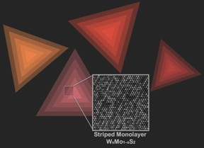 |
| This is an electron microscopy image of ordered atoms of tungsten (W) and molybdenum (Mo) against artistic representations of triangular single layer flakes of WxMo1-xS2 on a substrate. CREDIT Amin Azizi and Andrea Kohler/ Penn State |
Abstract:
By creating atomic chains in a two-dimensional crystal, researchers at Penn State believe they have found a way to control the direction of materials properties in two and three dimensional crystals with implications in sensing, optoelectronics and next-generation electronics applications.
Controlling the properties of matter in two-dimensional crystals
University Park, PA | Posted on November 8th, 2016Whether an alloy has a random arrangement of atoms or an arrangement that is ordered can have large effects on a material's properties. In a paper published online in Nano Letters, Nasim Alem, assistant professor of materials science and engineering, and colleagues at Penn State used a combination of simulations and scanning transmission electron microscopy (STEM) imaging to determine the atomic structure of an ordered alloy of molybdenum, tungsten and sulfur. They determined that fluctuations in the amount of available sulfur were responsible for the creation of atomic chains of either molybdenum or tungsten.
"We discovered how chains form in a two-dimensional alloy as a result of fluctuations in the amount of a particular precursor, in this case sulfur," said Alem. "Normally, when we combine atoms of different elements, we don't know how to control where the atoms will go. But we have found a mechanism to give order to the atoms, which in turn introduces control of the properties, not only heat transport, as is the case in this work, but also electronic, chemical or magnetic properties in other alloy cases. If you know the mechanism, you can apply it to arrange the atoms in a wide range of alloys in 2D crystals across the Periodic Table."
In the case of the molybdenum, tungsten and sulfur alloy, they showed that the electronic properties were the same in every direction, but using simulations they predict that the thermal transport properties are smaller perpendicular to the chains or stripes.
"We didn't know why this crystal forms an ordered structure, so we worked with my colleague Dr. Vin Crespi to understand the underlying physics that causes order in this crystal," said Alem. "Our calculations show it was the fluctuations in the third element, sulfur, that was determining how the chains formed."
Vincent H. Crespi, Distinguished Professor of Physics, and professor of chemistry and materials science and engineering who developed the theoretical understanding of the phenomenon, said, "Although the interior of the flake is indifferent to whether molybdenum or tungsten occupies any site in the crystal lattice, the edge of the growing crystal does care: Depending on how much sulfur is available at a given location, the edge will prefer to be either 100 percent molybdenum or 100 percent tungsten. So as the availability of sulfur randomly varies during growth, the system alternately lays down rows of molybdenum or tungsten. We think this may be a general mechanism to create stripe-like structures in 2D materials."
Amin Aziz, a Ph.D. candidate in Alem's group and lead author, produced the STEM imaging and spectroscopy that showed the fine atomic structure of the alloy samples and their electronic properties.
"When we are able to directly image constitutive atoms of a substance, see how they interact with each other at the atomic level and try to understand the origins of such behaviors, we could potentially create new materials with unusual properties that have never existed," said Azizi,
A team led by Mauricio Terrones, professor of physics, produced samples of this ordered alloy by vaporizing powders of all three elements, called precursors, under high heat.
###
Along with Azizi, Terrones, Alem and Crespi, other coauthors on the paper titled "Spontaneous formation of atomically thin stripes in transition metal dichalcogenide monolayers," include Yuanxi Wang, a Ph.D. candidate in Crespi's group, Ke Wang, a staff scientist in the Materials Research Institute who helped with the electron microscopy, Ph.D. candidate Zhong Lin in materials science and Ana Laura Elias, research associate in the Terrones group.
The National Science Foundation and the U.S. Army Research Office supported this work.
####
For more information, please click here
Contacts:
A'ndrea Elyse Messer
814-865-9481
Copyright © Penn State
If you have a comment, please Contact us.Issuers of news releases, not 7th Wave, Inc. or Nanotechnology Now, are solely responsible for the accuracy of the content.
Bookmark:


| Related News Press |
News and information
![]() Quantum computer improves AI predictions April 17th, 2026
Quantum computer improves AI predictions April 17th, 2026
![]() Flexible sensor gains sensitivity under pressure April 17th, 2026
Flexible sensor gains sensitivity under pressure April 17th, 2026
![]() A reusable chip for particulate matter sensing April 17th, 2026
A reusable chip for particulate matter sensing April 17th, 2026
![]() Detecting vibrational quantum beating in the predissociation dynamics of SF6 using time-resolved photoelectron spectroscopy April 17th, 2026
Detecting vibrational quantum beating in the predissociation dynamics of SF6 using time-resolved photoelectron spectroscopy April 17th, 2026
2 Dimensional Materials
![]() Flexible sensor gains sensitivity under pressure April 17th, 2026
Flexible sensor gains sensitivity under pressure April 17th, 2026
![]() MXene nanomaterials enter a new dimension Multilayer nanomaterial: MXene flakes created at Drexel University show new promise as 1D scrolls January 30th, 2026
MXene nanomaterials enter a new dimension Multilayer nanomaterial: MXene flakes created at Drexel University show new promise as 1D scrolls January 30th, 2026
Imaging
Govt.-Legislation/Regulation/Funding/Policy
![]() Quantum computer improves AI predictions April 17th, 2026
Quantum computer improves AI predictions April 17th, 2026
![]() Metasurfaces smooth light to boost magnetic sensing precision January 30th, 2026
Metasurfaces smooth light to boost magnetic sensing precision January 30th, 2026
![]() New imaging approach transforms study of bacterial biofilms August 8th, 2025
New imaging approach transforms study of bacterial biofilms August 8th, 2025
Possible Futures
![]() A fundamentally new therapeutic approach to cystic fibrosis: Nanobody repairs cellular defect April 17th, 2026
A fundamentally new therapeutic approach to cystic fibrosis: Nanobody repairs cellular defect April 17th, 2026
![]() UC Irvine physicists discover method to reverse �quantum scrambling� : The work addresses the problem of information loss in quantum computing system April 17th, 2026
UC Irvine physicists discover method to reverse �quantum scrambling� : The work addresses the problem of information loss in quantum computing system April 17th, 2026
Chip Technology
![]() A reusable chip for particulate matter sensing April 17th, 2026
A reusable chip for particulate matter sensing April 17th, 2026
![]() Metasurfaces smooth light to boost magnetic sensing precision January 30th, 2026
Metasurfaces smooth light to boost magnetic sensing precision January 30th, 2026
Optical computing/Photonic computing
![]() ICFO researchers overcome long-standing bottleneck in single photon detection with twisted 2D materials August 8th, 2025
ICFO researchers overcome long-standing bottleneck in single photon detection with twisted 2D materials August 8th, 2025
![]() Programmable electron-induced color router array May 14th, 2025
Programmable electron-induced color router array May 14th, 2025
Nanoelectronics
![]() Lab to industry: InSe wafer-scale breakthrough for future electronics August 8th, 2025
Lab to industry: InSe wafer-scale breakthrough for future electronics August 8th, 2025
![]() Interdisciplinary: Rice team tackles the future of semiconductors Multiferroics could be the key to ultralow-energy computing October 6th, 2023
Interdisciplinary: Rice team tackles the future of semiconductors Multiferroics could be the key to ultralow-energy computing October 6th, 2023
![]() Key element for a scalable quantum computer: Physicists from Forschungszentrum J�lich and RWTH Aachen University demonstrate electron transport on a quantum chip September 23rd, 2022
Key element for a scalable quantum computer: Physicists from Forschungszentrum J�lich and RWTH Aachen University demonstrate electron transport on a quantum chip September 23rd, 2022
![]() Reduced power consumption in semiconductor devices September 23rd, 2022
Reduced power consumption in semiconductor devices September 23rd, 2022
Discoveries
![]() Quantum computer improves AI predictions April 17th, 2026
Quantum computer improves AI predictions April 17th, 2026
![]() Flexible sensor gains sensitivity under pressure April 17th, 2026
Flexible sensor gains sensitivity under pressure April 17th, 2026
![]() A reusable chip for particulate matter sensing April 17th, 2026
A reusable chip for particulate matter sensing April 17th, 2026
![]() Detecting vibrational quantum beating in the predissociation dynamics of SF6 using time-resolved photoelectron spectroscopy April 17th, 2026
Detecting vibrational quantum beating in the predissociation dynamics of SF6 using time-resolved photoelectron spectroscopy April 17th, 2026
Materials/Metamaterials/Magnetoresistance
![]() First real-time observation of two-dimensional melting process: Researchers at Mainz University unveil new insights into magnetic vortex structures August 8th, 2025
First real-time observation of two-dimensional melting process: Researchers at Mainz University unveil new insights into magnetic vortex structures August 8th, 2025
![]() Researchers unveil a groundbreaking clay-based solution to capture carbon dioxide and combat climate change June 6th, 2025
Researchers unveil a groundbreaking clay-based solution to capture carbon dioxide and combat climate change June 6th, 2025
![]() A 1960s idea inspires NBI researchers to study hitherto inaccessible quantum states June 6th, 2025
A 1960s idea inspires NBI researchers to study hitherto inaccessible quantum states June 6th, 2025
![]() Institute for Nanoscience hosts annual proposal planning meeting May 16th, 2025
Institute for Nanoscience hosts annual proposal planning meeting May 16th, 2025
Announcements
![]() A fundamentally new therapeutic approach to cystic fibrosis: Nanobody repairs cellular defect April 17th, 2026
A fundamentally new therapeutic approach to cystic fibrosis: Nanobody repairs cellular defect April 17th, 2026
![]() UC Irvine physicists discover method to reverse �quantum scrambling� : The work addresses the problem of information loss in quantum computing system April 17th, 2026
UC Irvine physicists discover method to reverse �quantum scrambling� : The work addresses the problem of information loss in quantum computing system April 17th, 2026
Interviews/Book Reviews/Essays/Reports/Podcasts/Journals/White papers/Posters
![]() A fundamentally new therapeutic approach to cystic fibrosis: Nanobody repairs cellular defect April 17th, 2026
A fundamentally new therapeutic approach to cystic fibrosis: Nanobody repairs cellular defect April 17th, 2026
![]() UC Irvine physicists discover method to reverse �quantum scrambling� : The work addresses the problem of information loss in quantum computing system April 17th, 2026
UC Irvine physicists discover method to reverse �quantum scrambling� : The work addresses the problem of information loss in quantum computing system April 17th, 2026
Tools
![]() Metasurfaces smooth light to boost magnetic sensing precision January 30th, 2026
Metasurfaces smooth light to boost magnetic sensing precision January 30th, 2026
![]() From sensors to smart systems: the rise of AI-driven photonic noses January 30th, 2026
From sensors to smart systems: the rise of AI-driven photonic noses January 30th, 2026
![]() Japan launches fully domestically produced quantum computer: Expo visitors to experience quantum computing firsthand August 8th, 2025
Japan launches fully domestically produced quantum computer: Expo visitors to experience quantum computing firsthand August 8th, 2025
Military
![]() Quantum engineers �squeeze� laser frequency combs to make more sensitive gas sensors January 17th, 2025
Quantum engineers �squeeze� laser frequency combs to make more sensitive gas sensors January 17th, 2025
![]() Chainmail-like material could be the future of armor: First 2D mechanically interlocked polymer exhibits exceptional flexibility and strength January 17th, 2025
Chainmail-like material could be the future of armor: First 2D mechanically interlocked polymer exhibits exceptional flexibility and strength January 17th, 2025
![]() Single atoms show their true color July 5th, 2024
Single atoms show their true color July 5th, 2024
![]() NRL charters Navy�s quantum inertial navigation path to reduce drift April 5th, 2024
NRL charters Navy�s quantum inertial navigation path to reduce drift April 5th, 2024
Photonics/Optics/Lasers
![]() Metasurfaces smooth light to boost magnetic sensing precision January 30th, 2026
Metasurfaces smooth light to boost magnetic sensing precision January 30th, 2026
![]() From sensors to smart systems: the rise of AI-driven photonic noses January 30th, 2026
From sensors to smart systems: the rise of AI-driven photonic noses January 30th, 2026
|
|
||
|
|
||
| The latest news from around the world, FREE | ||
|
|
||
|
|
||
| Premium Products | ||
|
|
||
|
Only the news you want to read!
Learn More |
||
|
|
||
|
Full-service, expert consulting
Learn More |
||
|
|
||