Home > Press > Device to control 'color' of electrons in graphene provides path to future electronics
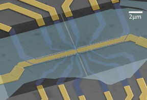 |
| This is a scanned electron micrograph of a device used in this experiment. Thin sheets of graphene and hexagonal Boron Nitride are stacked and shaped by electron beam lithography to create this device. The purple layer is the bilayer graphene sheet. The bottom pair of split gates (dark squares) are made of multi-layer graphene. The top pair of split gates (gold bars) are made of gold. The one-dimensional wires live in the gap created by the split gates. CREDIT: Zhu, Penn State |
Abstract:
A device made of bilayer graphene, an atomically thin hexagonal arrangement of carbon atoms, provides experimental proof of the ability to control the momentum of electrons and offers a path to electronics that could require less energy and give off less heat than standard silicon-based transistors. It is one step forward in a new field of physics called valleytronics.
Device to control 'color' of electrons in graphene provides path to future electronics
University Park, PA | Posted on August 31st, 2016"Current silicon-based transistor devices rely on the charge of electrons to turn the device on or off, but many labs are looking at new ways to manipulate electrons based on other variables, called degrees of freedom," said Jun Zhu, associate professor of physics, Penn State, who directed the research. "Charge is one degree of freedom. Electron spin is another, and the ability to build transistors based on spin, called spintronics, is still in the development stage. A third electronic degree of freedom is the valley state of electrons, which is based on their energy in relation to their momentum."
Think of electrons as cars and the valley states as blue and red colors, Zhu suggested, just as a way to differentiate them. Inside a sheet of bilayer graphene, electrons will normally occupy both red and blue valley states and travel in all directions. The device her Ph.D. student, Jing Li, has been working on can make the red cars go in one direction and the blue cars in the opposite direction.
"The system that Jing created puts a pair of gates above and below a bilayer graphene sheet. Then he adds an electric field perpendicular to the plane," Zhu said.
"By applying a positive voltage on one side and a negative voltage on the other, a bandgap opens in bilayer graphene, which it doesn't normally have," Li explained. "In the middle, between the two sides, we leave a physical gap of about 70 nanometers."
Inside this gap live one-dimensional metallic states, or wires, that are color-coded freeways for electrons. The red cars travel in one direction and the blue cars travel in the opposite direction. In theory, colored electrons could travel unhindered along the wires for a long distance with very little resistance. Smaller resistance means power consumption is lower in electronic devices and less heat is generated. Both power consumption and thermal management are challenges in current miniaturized devices.
"Our experiments show that the metallic wires can be created," Li said. "Although we are still a long way from applications."
Zhu added, "It's quite remarkable that such states can be created in the interior of an insulating bilayer graphene sheet, using just a few gates. They are not yet resistance-free, and we are doing more experiments to understand where resistance might come from. We are also trying to build valves that control the electron flow based on the color of the electrons. That's a new concept of electronics called valleytronics."
Li worked closely with the technical staff of Penn State's nanofabrication facility to turn the theoretical framework into a working device.
"The alignment of the top and bottom gates was crucial and not a trivial challenge," said Chad Eichfeld, nanolithography engineer. "The state-of-the-art electron beam lithography capabilities at the Penn State Nanofabrication Laboratory allowed Jing to create this novel device with nanoscale features."
###
Their paper, "Gate-controlled topological conducting channels in bilayer graphene," appears online today (Aug 29) in the journal Nature Nanotechnology. Additional authors include Ke Wang and Yafei Ren and their advisor Zenhua Qiao of University of Science and Technology of China, who performed numerical studies to model the behavior of the wires. The high-quality hexagonal Boron Nitride crystals used in the experiment came from Kenji Watanabe and Takashi Taniguchi of National Institute for Material Science, Japan. Two undergraduate students, Kenton McFaul and Zachary Zern, contributed to the research.
The U.S. Office of Naval Research, the National Science Foundation and funding agencies in China and Japan funded this project. Kenton McFaul, a visiting student from Grove City College, was supported by a Research Experience for Undergraduates grant from the NSF NNIN. Jun Zhu is a member of the Center for 2-Dimensional and Layered Materials in Penn State's Materials Research Institute.
####
For more information, please click here
Contacts:
A'ndrea Elyse Messer
814-865-9481
Copyright © Penn State
If you have a comment, please Contact us.Issuers of news releases, not 7th Wave, Inc. or Nanotechnology Now, are solely responsible for the accuracy of the content.
Bookmark:


| Related Links |
| Related News Press |
News and information
![]() Quantum computer improves AI predictions April 17th, 2026
Quantum computer improves AI predictions April 17th, 2026
![]() Flexible sensor gains sensitivity under pressure April 17th, 2026
Flexible sensor gains sensitivity under pressure April 17th, 2026
![]() A reusable chip for particulate matter sensing April 17th, 2026
A reusable chip for particulate matter sensing April 17th, 2026
![]() Detecting vibrational quantum beating in the predissociation dynamics of SF6 using time-resolved photoelectron spectroscopy April 17th, 2026
Detecting vibrational quantum beating in the predissociation dynamics of SF6 using time-resolved photoelectron spectroscopy April 17th, 2026
2 Dimensional Materials
![]() Flexible sensor gains sensitivity under pressure April 17th, 2026
Flexible sensor gains sensitivity under pressure April 17th, 2026
Graphene/ Graphite
![]() Electrifying results shed light on graphene foam as a potential material for lab grown cartilage June 6th, 2025
Electrifying results shed light on graphene foam as a potential material for lab grown cartilage June 6th, 2025
![]() Breakthrough in proton barrier films using pore-free graphene oxide: Kumamoto University researchers achieve new milestone in advanced coating technologies September 13th, 2024
Breakthrough in proton barrier films using pore-free graphene oxide: Kumamoto University researchers achieve new milestone in advanced coating technologies September 13th, 2024
Govt.-Legislation/Regulation/Funding/Policy
![]() Quantum computer improves AI predictions April 17th, 2026
Quantum computer improves AI predictions April 17th, 2026
![]() Metasurfaces smooth light to boost magnetic sensing precision January 30th, 2026
Metasurfaces smooth light to boost magnetic sensing precision January 30th, 2026
![]() New imaging approach transforms study of bacterial biofilms August 8th, 2025
New imaging approach transforms study of bacterial biofilms August 8th, 2025
Possible Futures
![]() A fundamentally new therapeutic approach to cystic fibrosis: Nanobody repairs cellular defect April 17th, 2026
A fundamentally new therapeutic approach to cystic fibrosis: Nanobody repairs cellular defect April 17th, 2026
![]() UC Irvine physicists discover method to reverse �quantum scrambling� : The work addresses the problem of information loss in quantum computing system April 17th, 2026
UC Irvine physicists discover method to reverse �quantum scrambling� : The work addresses the problem of information loss in quantum computing system April 17th, 2026
Chip Technology
![]() A reusable chip for particulate matter sensing April 17th, 2026
A reusable chip for particulate matter sensing April 17th, 2026
![]() Metasurfaces smooth light to boost magnetic sensing precision January 30th, 2026
Metasurfaces smooth light to boost magnetic sensing precision January 30th, 2026
Discoveries
![]() Quantum computer improves AI predictions April 17th, 2026
Quantum computer improves AI predictions April 17th, 2026
![]() Flexible sensor gains sensitivity under pressure April 17th, 2026
Flexible sensor gains sensitivity under pressure April 17th, 2026
![]() A reusable chip for particulate matter sensing April 17th, 2026
A reusable chip for particulate matter sensing April 17th, 2026
![]() Detecting vibrational quantum beating in the predissociation dynamics of SF6 using time-resolved photoelectron spectroscopy April 17th, 2026
Detecting vibrational quantum beating in the predissociation dynamics of SF6 using time-resolved photoelectron spectroscopy April 17th, 2026
Materials/Metamaterials/Magnetoresistance
![]() First real-time observation of two-dimensional melting process: Researchers at Mainz University unveil new insights into magnetic vortex structures August 8th, 2025
First real-time observation of two-dimensional melting process: Researchers at Mainz University unveil new insights into magnetic vortex structures August 8th, 2025
![]() Researchers unveil a groundbreaking clay-based solution to capture carbon dioxide and combat climate change June 6th, 2025
Researchers unveil a groundbreaking clay-based solution to capture carbon dioxide and combat climate change June 6th, 2025
![]() A 1960s idea inspires NBI researchers to study hitherto inaccessible quantum states June 6th, 2025
A 1960s idea inspires NBI researchers to study hitherto inaccessible quantum states June 6th, 2025
![]() Institute for Nanoscience hosts annual proposal planning meeting May 16th, 2025
Institute for Nanoscience hosts annual proposal planning meeting May 16th, 2025
Announcements
![]() A fundamentally new therapeutic approach to cystic fibrosis: Nanobody repairs cellular defect April 17th, 2026
A fundamentally new therapeutic approach to cystic fibrosis: Nanobody repairs cellular defect April 17th, 2026
![]() UC Irvine physicists discover method to reverse �quantum scrambling� : The work addresses the problem of information loss in quantum computing system April 17th, 2026
UC Irvine physicists discover method to reverse �quantum scrambling� : The work addresses the problem of information loss in quantum computing system April 17th, 2026
Interviews/Book Reviews/Essays/Reports/Podcasts/Journals/White papers/Posters
![]() A fundamentally new therapeutic approach to cystic fibrosis: Nanobody repairs cellular defect April 17th, 2026
A fundamentally new therapeutic approach to cystic fibrosis: Nanobody repairs cellular defect April 17th, 2026
![]() UC Irvine physicists discover method to reverse �quantum scrambling� : The work addresses the problem of information loss in quantum computing system April 17th, 2026
UC Irvine physicists discover method to reverse �quantum scrambling� : The work addresses the problem of information loss in quantum computing system April 17th, 2026
Military
![]() Quantum engineers �squeeze� laser frequency combs to make more sensitive gas sensors January 17th, 2025
Quantum engineers �squeeze� laser frequency combs to make more sensitive gas sensors January 17th, 2025
![]() Chainmail-like material could be the future of armor: First 2D mechanically interlocked polymer exhibits exceptional flexibility and strength January 17th, 2025
Chainmail-like material could be the future of armor: First 2D mechanically interlocked polymer exhibits exceptional flexibility and strength January 17th, 2025
![]() Single atoms show their true color July 5th, 2024
Single atoms show their true color July 5th, 2024
![]() NRL charters Navy�s quantum inertial navigation path to reduce drift April 5th, 2024
NRL charters Navy�s quantum inertial navigation path to reduce drift April 5th, 2024
Research partnerships
![]() Lab to industry: InSe wafer-scale breakthrough for future electronics August 8th, 2025
Lab to industry: InSe wafer-scale breakthrough for future electronics August 8th, 2025
![]() HKU physicists uncover hidden order in the quantum world through deconfined quantum critical points April 25th, 2025
HKU physicists uncover hidden order in the quantum world through deconfined quantum critical points April 25th, 2025
|
|
||
|
|
||
| The latest news from around the world, FREE | ||
|
|
||
|
|
||
| Premium Products | ||
|
|
||
|
Only the news you want to read!
Learn More |
||
|
|
||
|
Full-service, expert consulting
Learn More |
||
|
|
||