Home > Press > See-through circuitry: New method makes AZO a viable and cheap alternative for transparent electronics
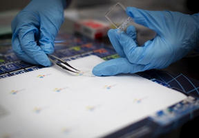 |
| KAUST researchers formed transparent electronic circuits on flexible plastic surfaces.
� 2016 KAUST |
Abstract:
High-performance electronic circuits made entirely from transparent materials could have countless applications, from head-up displays on car windscreens to transparent TV sets and smart windows in homes and offices. Researchers at KAUST have found a way to make transparent transistors and other essential components of electronic circuitry using inexpensive and readily available materials and a simple fabrication technique1.
See-through circuitry: New method makes AZO a viable and cheap alternative for transparent electronics
Thuwal, Saudi Arabia | Posted on August 15th, 2016Indium tin oxide (ITO) is the current material of choice for electronics because it combines optical transparency with electrical conductivity. Its use ranges from touch-sensitive smartphone screens to light-harvesting solar panels. Indium is in short supply, however, and as demand increases for ITO-containing devices, so does the price of indium.
One promising low-cost ITO alternative is a transparent material known as aluminum-doped zinc oxide (AZO).
"The elements that make up this material are more abundant than indium, making AZO a commercially sensible option," said Professor Husam Alshareef from the KAUST Physical Science and Engineering Division who also led the research. "However, electronic devices made using AZO have traditionally shown inferior performance to devices made using ITO."
To overcome this limitation, Alshareef and his research team used a high-precision technology called atomic layer deposition, a process in which the circuitry is built up a single layer of atoms at a time. Volatile vapors of aluminum and zinc in the form of trimethyl aluminum and diethyl zinc were alternately introduced onto the transparent substrate, where they adhere to the surface in a single layer before reacting in situ to form AZO.
"Using atomic layer deposition to grow all active layers simplifies the circuit fabrication process and significantly improves circuit performance by controlling layer growth at the atomic scale," Alshareef explained.
For many electronic devices, the key component is the thin film transistor. When combined in great numbers, these devices allow computers to do calculations, drive displays and act as active sensors. Alshareef used a transparent material called hafnium oxide that was sandwiched between layers of zinc oxide to form the highly-stable transistors used to fabricate the transparent circuits.
"Our transistor properties are the best reported so far for fully transparent transistors using AZO contacts," said Ph.D. student Zhenwei Wang, who carried out much of the experimental work.
Another advantage of Alshareef's approach is that atomic layer deposition only requires a temperature of 160 degrees Celsius to form each layer, which is low enough for the transparent circuitry to be formed on flexible plastic substrates as well as on rigid glass.
####
For more information, please click here
Contacts:
Michelle D'Antoni
Copyright © King Abdullah University of Science and Technology
If you have a comment, please Contact us.Issuers of news releases, not 7th Wave, Inc. or Nanotechnology Now, are solely responsible for the accuracy of the content.
Bookmark:


| Related Links |
| Related News Press |
News and information
![]() Quantum computer improves AI predictions April 17th, 2026
Quantum computer improves AI predictions April 17th, 2026
![]() Flexible sensor gains sensitivity under pressure April 17th, 2026
Flexible sensor gains sensitivity under pressure April 17th, 2026
![]() A reusable chip for particulate matter sensing April 17th, 2026
A reusable chip for particulate matter sensing April 17th, 2026
![]() Detecting vibrational quantum beating in the predissociation dynamics of SF6 using time-resolved photoelectron spectroscopy April 17th, 2026
Detecting vibrational quantum beating in the predissociation dynamics of SF6 using time-resolved photoelectron spectroscopy April 17th, 2026
Flexible Electronics
![]() Flexible sensor gains sensitivity under pressure April 17th, 2026
Flexible sensor gains sensitivity under pressure April 17th, 2026
Chip Technology
![]() A reusable chip for particulate matter sensing April 17th, 2026
A reusable chip for particulate matter sensing April 17th, 2026
![]() Metasurfaces smooth light to boost magnetic sensing precision January 30th, 2026
Metasurfaces smooth light to boost magnetic sensing precision January 30th, 2026
Discoveries
![]() Quantum computer improves AI predictions April 17th, 2026
Quantum computer improves AI predictions April 17th, 2026
![]() Flexible sensor gains sensitivity under pressure April 17th, 2026
Flexible sensor gains sensitivity under pressure April 17th, 2026
![]() A reusable chip for particulate matter sensing April 17th, 2026
A reusable chip for particulate matter sensing April 17th, 2026
![]() Detecting vibrational quantum beating in the predissociation dynamics of SF6 using time-resolved photoelectron spectroscopy April 17th, 2026
Detecting vibrational quantum beating in the predissociation dynamics of SF6 using time-resolved photoelectron spectroscopy April 17th, 2026
Materials/Metamaterials/Magnetoresistance
![]() First real-time observation of two-dimensional melting process: Researchers at Mainz University unveil new insights into magnetic vortex structures August 8th, 2025
First real-time observation of two-dimensional melting process: Researchers at Mainz University unveil new insights into magnetic vortex structures August 8th, 2025
![]() Researchers unveil a groundbreaking clay-based solution to capture carbon dioxide and combat climate change June 6th, 2025
Researchers unveil a groundbreaking clay-based solution to capture carbon dioxide and combat climate change June 6th, 2025
![]() A 1960s idea inspires NBI researchers to study hitherto inaccessible quantum states June 6th, 2025
A 1960s idea inspires NBI researchers to study hitherto inaccessible quantum states June 6th, 2025
![]() Institute for Nanoscience hosts annual proposal planning meeting May 16th, 2025
Institute for Nanoscience hosts annual proposal planning meeting May 16th, 2025
Announcements
![]() A fundamentally new therapeutic approach to cystic fibrosis: Nanobody repairs cellular defect April 17th, 2026
A fundamentally new therapeutic approach to cystic fibrosis: Nanobody repairs cellular defect April 17th, 2026
![]() UC Irvine physicists discover method to reverse �quantum scrambling� : The work addresses the problem of information loss in quantum computing system April 17th, 2026
UC Irvine physicists discover method to reverse �quantum scrambling� : The work addresses the problem of information loss in quantum computing system April 17th, 2026
Interviews/Book Reviews/Essays/Reports/Podcasts/Journals/White papers/Posters
![]() A fundamentally new therapeutic approach to cystic fibrosis: Nanobody repairs cellular defect April 17th, 2026
A fundamentally new therapeutic approach to cystic fibrosis: Nanobody repairs cellular defect April 17th, 2026
![]() UC Irvine physicists discover method to reverse �quantum scrambling� : The work addresses the problem of information loss in quantum computing system April 17th, 2026
UC Irvine physicists discover method to reverse �quantum scrambling� : The work addresses the problem of information loss in quantum computing system April 17th, 2026
Tools
![]() Metasurfaces smooth light to boost magnetic sensing precision January 30th, 2026
Metasurfaces smooth light to boost magnetic sensing precision January 30th, 2026
![]() From sensors to smart systems: the rise of AI-driven photonic noses January 30th, 2026
From sensors to smart systems: the rise of AI-driven photonic noses January 30th, 2026
![]() Japan launches fully domestically produced quantum computer: Expo visitors to experience quantum computing firsthand August 8th, 2025
Japan launches fully domestically produced quantum computer: Expo visitors to experience quantum computing firsthand August 8th, 2025
|
|
||
|
|
||
| The latest news from around the world, FREE | ||
|
|
||
|
|
||
| Premium Products | ||
|
|
||
|
Only the news you want to read!
Learn More |
||
|
|
||
|
Full-service, expert consulting
Learn More |
||
|
|
||