Home > Press > NUS scientists develop novel method to improve photoluminescence efficiency of two-dimensional semiconductors
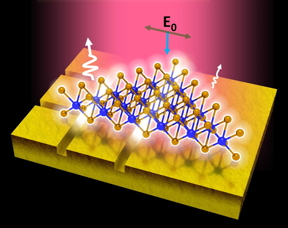 |
| This is a schematic of the light emission from a single crystal monolayer of
tungsten diselenide flake on a gold substrate. Part of the triangular flake rests
on the patterned region of the substrate consisting of sub-20 nm wide trenches.
Photo Credit: Andrew T. S. Wee |
Abstract:
A team led by researchers from the National University of Singapore (NUS) has developed a method to enhance the photoluminescence efficiency of tungsten diselenide, a two-dimensional semiconductor, paving the way for the application of such semiconductors in advanced optoelectronic and photonic devices.
NUS scientists develop novel method to improve photoluminescence efficiency of two-dimensional semiconductors
Singapore | Posted on May 9th, 2016Tungsten diselenide is a single-molecule-thick semiconductor that is part of an emerging class of materials called transition metal dichalcogenides (TMDCs), which have the ability to convert light to electricity and vice versa, making them strong potential candidates for optoelectronic devices such as thin film solar cells, photodetectors flexible logic circuits and sensors. However, its atomically thin structure reduces its absorption and photoluminescence properties, thereby limiting its practical applications.
By incorporating monolayers of tungsten diselenide onto gold substrates with nanosized trenches, the research team, led by Professor Andrew Wee of the Department of Physics at the NUS Faculty of Science, successfully enhanced the nanomaterial�s photoluminescence by up to 20,000-fold. This technological breakthrough creates new opportunities of applying tungsten diselenide as a novel semiconductor material for advanced applications.
Ms Wang Zhuo, a PhD candidate from the NUS Graduate School for Integrative Sciences and Engineering (NGS) and first author of the paper, explained, �This is the first work to demonstrate the use of gold plasmonic nanostructures to improve the photoluminescence of tungsten diselenide, and we have managed to achieve an unprecedented enhancement of the light absorption and emission efficiency of this nanomaterial.�
Elaborating on the significance of the novel method, Prof Wee said, �The key to this work is the design of the gold plasmonic nanoarray templates. In our system, the resonances can be tuned to be matched with the pump laser wavelength by varying the pitch of the structures. This is critical for plasmon coupling with light to achieve optimal field confinement.�
The novel research was first published online in the journal Nature Communications on 7 May 2016.
The next step
The novel method developed by the NUS team, in collaboration with researchers from the Singapore University of Technology and Design and Imperial College, opens up a new platform for investigating novel electrical and optical properties in the hybrid system of gold with tungsten diselenide. Moving forward, the research team will further investigate the effectiveness of the lateral gold plasmon in enhancing the second harmonic generation and electroluminescence of TMDCs. They will also investigate these effects in other two dimensional transition metal dichalcogenides with different band gaps, as they are expected to show different interaction mechanisms.
####
About National University of Singapore (NUS)
A leading global university centred in Asia, the National University of Singapore (NUS) is Singapore�s flagship university, which offers a global approach to education and research, with a focus on Asian perspectives and expertise.
NUS has 17 faculties and schools across three campuses. Its transformative education includes a broad-based curriculum underscored by multi-disciplinary courses and cross-faculty enrichment. Over 38,000 students from 100 countries enrich the community with their diverse social and cultural perspectives.
NUS has three Research Centres of Excellence (RCE) and 26 university-level research institutes and centres. It is also a partner in Singapore�s fifth RCE. NUS shares a close affiliation with 16 national-level research institutes and centres. Research activities are strategic and robust, and NUS is well-known for its research strengths in engineering, life sciences and biomedicine, social sciences and natural sciences. It also strives to create a supportive and innovative environment to promote creative enterprise within its community.
For more information, please click here
Contacts:
Carolyn FONG
Associate Director, Media Relations
Office of Corporate Relations
National University of Singapore
DID: +65 6516 5399
Copyright © National University of Singapore (NUS)
If you have a comment, please Contact us.Issuers of news releases, not 7th Wave, Inc. or Nanotechnology Now, are solely responsible for the accuracy of the content.
Bookmark:


| Related News Press |
News and information
![]() Quantum computer improves AI predictions April 17th, 2026
Quantum computer improves AI predictions April 17th, 2026
![]() Flexible sensor gains sensitivity under pressure April 17th, 2026
Flexible sensor gains sensitivity under pressure April 17th, 2026
![]() A reusable chip for particulate matter sensing April 17th, 2026
A reusable chip for particulate matter sensing April 17th, 2026
![]() Detecting vibrational quantum beating in the predissociation dynamics of SF6 using time-resolved photoelectron spectroscopy April 17th, 2026
Detecting vibrational quantum beating in the predissociation dynamics of SF6 using time-resolved photoelectron spectroscopy April 17th, 2026
2 Dimensional Materials
![]() Flexible sensor gains sensitivity under pressure April 17th, 2026
Flexible sensor gains sensitivity under pressure April 17th, 2026
Possible Futures
![]() A fundamentally new therapeutic approach to cystic fibrosis: Nanobody repairs cellular defect April 17th, 2026
A fundamentally new therapeutic approach to cystic fibrosis: Nanobody repairs cellular defect April 17th, 2026
![]() UC Irvine physicists discover method to reverse �quantum scrambling� : The work addresses the problem of information loss in quantum computing system April 17th, 2026
UC Irvine physicists discover method to reverse �quantum scrambling� : The work addresses the problem of information loss in quantum computing system April 17th, 2026
Chip Technology
![]() A reusable chip for particulate matter sensing April 17th, 2026
A reusable chip for particulate matter sensing April 17th, 2026
![]() Metasurfaces smooth light to boost magnetic sensing precision January 30th, 2026
Metasurfaces smooth light to boost magnetic sensing precision January 30th, 2026
Optical computing/Photonic computing
![]() ICFO researchers overcome long-standing bottleneck in single photon detection with twisted 2D materials August 8th, 2025
ICFO researchers overcome long-standing bottleneck in single photon detection with twisted 2D materials August 8th, 2025
![]() Programmable electron-induced color router array May 14th, 2025
Programmable electron-induced color router array May 14th, 2025
Nanoelectronics
![]() Lab to industry: InSe wafer-scale breakthrough for future electronics August 8th, 2025
Lab to industry: InSe wafer-scale breakthrough for future electronics August 8th, 2025
![]() Interdisciplinary: Rice team tackles the future of semiconductors Multiferroics could be the key to ultralow-energy computing October 6th, 2023
Interdisciplinary: Rice team tackles the future of semiconductors Multiferroics could be the key to ultralow-energy computing October 6th, 2023
![]() Key element for a scalable quantum computer: Physicists from Forschungszentrum J�lich and RWTH Aachen University demonstrate electron transport on a quantum chip September 23rd, 2022
Key element for a scalable quantum computer: Physicists from Forschungszentrum J�lich and RWTH Aachen University demonstrate electron transport on a quantum chip September 23rd, 2022
![]() Reduced power consumption in semiconductor devices September 23rd, 2022
Reduced power consumption in semiconductor devices September 23rd, 2022
Discoveries
![]() Quantum computer improves AI predictions April 17th, 2026
Quantum computer improves AI predictions April 17th, 2026
![]() Flexible sensor gains sensitivity under pressure April 17th, 2026
Flexible sensor gains sensitivity under pressure April 17th, 2026
![]() A reusable chip for particulate matter sensing April 17th, 2026
A reusable chip for particulate matter sensing April 17th, 2026
![]() Detecting vibrational quantum beating in the predissociation dynamics of SF6 using time-resolved photoelectron spectroscopy April 17th, 2026
Detecting vibrational quantum beating in the predissociation dynamics of SF6 using time-resolved photoelectron spectroscopy April 17th, 2026
Announcements
![]() A fundamentally new therapeutic approach to cystic fibrosis: Nanobody repairs cellular defect April 17th, 2026
A fundamentally new therapeutic approach to cystic fibrosis: Nanobody repairs cellular defect April 17th, 2026
![]() UC Irvine physicists discover method to reverse �quantum scrambling� : The work addresses the problem of information loss in quantum computing system April 17th, 2026
UC Irvine physicists discover method to reverse �quantum scrambling� : The work addresses the problem of information loss in quantum computing system April 17th, 2026
Interviews/Book Reviews/Essays/Reports/Podcasts/Journals/White papers/Posters
![]() A fundamentally new therapeutic approach to cystic fibrosis: Nanobody repairs cellular defect April 17th, 2026
A fundamentally new therapeutic approach to cystic fibrosis: Nanobody repairs cellular defect April 17th, 2026
![]() UC Irvine physicists discover method to reverse �quantum scrambling� : The work addresses the problem of information loss in quantum computing system April 17th, 2026
UC Irvine physicists discover method to reverse �quantum scrambling� : The work addresses the problem of information loss in quantum computing system April 17th, 2026
Photonics/Optics/Lasers
![]() Metasurfaces smooth light to boost magnetic sensing precision January 30th, 2026
Metasurfaces smooth light to boost magnetic sensing precision January 30th, 2026
![]() From sensors to smart systems: the rise of AI-driven photonic noses January 30th, 2026
From sensors to smart systems: the rise of AI-driven photonic noses January 30th, 2026
|
|
||
|
|
||
| The latest news from around the world, FREE | ||
|
|
||
|
|
||
| Premium Products | ||
|
|
||
|
Only the news you want to read!
Learn More |
||
|
|
||
|
Full-service, expert consulting
Learn More |
||
|
|
||