Home > Press > Exploring phosphorene, a promising new material
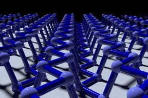 |
| Phosphorene, a single layer of phosphorous in a particular configuration, has potential application in semiconductor transistors. CREDIT: Matthew Cherny |
Abstract:
Two-dimensional phosphane, a material known as phosphorene, has potential application as a material for semiconducting transistors in ever faster and more powerful computers. But there's a hitch. Many of the useful properties of this material, like its ability to conduct electrons, are anisotropic, meaning they vary depending on the orientation of the crystal. Now, a team including researchers at Rensselaer Polytechnic Institute (RPI) has developed a new method to quickly and accurately determine that orientation using the interactions between light and electrons within phosphorene and other atoms-thick crystals of black phosphorus.
Exploring phosphorene, a promising new material
Troy, NY | Posted on April 29th, 2016Phosphorene--a single layer of phosphorous atoms--was isolated for the first time in 2014, allowing physicists to begin exploring its properties experimentally and theoretically. Vincent Meunier, head of the Rensselaer Department of Physics, Applied Physics, and Astronomy and a leader of the team that developed the new method, published his first paper on the material--confirming the structure of phosphorene--in that same year.
"This is a really interesting material because, depending on which direction you do things, you have completely different properties," said Meunier, a member of the Rensselaer Center for Materials, Devices, and Integrated Systems (cMDIS). "But because it's such a new material, it's essential that we begin to understand and predict its intrinsic properties."
Meunier and researchers at Rensselaer contributed to the theoretical modeling and prediction of the properties of phosphorene, drawing on the Rensselaer supercomputer, the Center for Computational Innovations (CCI), to perform calculations. Through the Rensselaer cMDIS, Meunier and his team are able to develop the potential of new materials such as phosphorene to serve in future generations of computers and other devices. Meunier's research exemplifies the work being done at The New Polytechnic, addressing difficult and complex global challenges, the need for interdisciplinary and true collaboration, and the use of the latest tools and technologies, many of which are developed at Rensselaer.
In their research, which appears in ACS Nano Letters, the team initially set out to refine an existing technique for determining the orientation of the crystal. This technique, which takes advantage of Raman spectroscopy, uses a laser to measure vibrations of the atoms within the crystal as energy moves through it, caused by electron-phonon interactions. Like other interactions, electron-phonon interactions within atoms-thick crystals of black phosphorus are anisotropic and, once measured, have been used to predict the orientation of the crystal.
In reviewing their initial results from Raman spectroscopy, the team noticed several inconsistencies. To investigate further, they obtained actual images of the orientation of their sample crystals using Transmission Electron Microscopy (TEM), and then compared them with the Raman spectroscopy results. As a topographic technique, TEM offers a definitive determination of the orientation of the crystal, but isn't as easy to obtain as the Raman results. The comparison revealed that electron-phonon interactions alone did not accurately predict the orientation of the crystal. And the reason why led the way to yet another anisotropy of phosphorene--that of interactions between photons of light and electrons in the crystal.
"In Raman you use a laser to impart energy into the material, and it starts to vibrate in ways that are intrinsic to the material, and which, in phosphorene, are anisotropic," said Meunier. "But it turns out that if you shine the light in different directions, you get different results, because the interaction between the light and the electrons in the material--the electron-photon interaction--is also anisotropic, but in a non-commensurate way."
Meunier said the team had reason to believe phosphorene was anisotropic with respect to electron-photon interactions, but didn't anticipate the importance of the property.
"Usually electron-photon anisotropy doesn't make such a big difference, but here, because we have such a particular chemistry on the surface and such a strong anisotropy, it's one of those materials where it makes a huge difference," Meunier said.
Although the discovery revealed a flaw in the interpretations of Raman spectra relying on electron-phonon interactions, it also revealed that electron-photon interactions alone provide an accurate determination of the orientation of the crystal.
"It turns out that it's not so easy to use Raman vibrations to find out the direction of the crystal," Meunier said. "But, and this is the beautiful thing, what we found is that the electron-photon interaction (which can be measured by recording the amount of light absorbed)--the interaction between the electrons and the laser--is a good predictor of the direction. Now you can really predict how the material will behave as a function of excitement with an outside stimulus."
###
The research, "Anisotropic Electron-Photon and Electron-Phonon Interactions in Black Phosphorus," was led by Meunier and Mildred Dresselhaus at Massachusetts Institute of Technology, and included researchers at Tohoku University in Japan, Oak Ridge National Laboratory, and the University of Pennsylvania, as well as Rensselaer.
####
For more information, please click here
Contacts:
Mary Martialay
Copyright © Rensselaer Polytechnic Institute
If you have a comment, please Contact us.Issuers of news releases, not 7th Wave, Inc. or Nanotechnology Now, are solely responsible for the accuracy of the content.
Bookmark:


| Related News Press |
News and information
![]() Quantum computer improves AI predictions April 17th, 2026
Quantum computer improves AI predictions April 17th, 2026
![]() Flexible sensor gains sensitivity under pressure April 17th, 2026
Flexible sensor gains sensitivity under pressure April 17th, 2026
![]() A reusable chip for particulate matter sensing April 17th, 2026
A reusable chip for particulate matter sensing April 17th, 2026
![]() Detecting vibrational quantum beating in the predissociation dynamics of SF6 using time-resolved photoelectron spectroscopy April 17th, 2026
Detecting vibrational quantum beating in the predissociation dynamics of SF6 using time-resolved photoelectron spectroscopy April 17th, 2026
2 Dimensional Materials
![]() Flexible sensor gains sensitivity under pressure April 17th, 2026
Flexible sensor gains sensitivity under pressure April 17th, 2026
![]() ICFO researchers overcome long-standing bottleneck in single photon detection with twisted 2D materials August 8th, 2025
ICFO researchers overcome long-standing bottleneck in single photon detection with twisted 2D materials August 8th, 2025
![]() First real-time observation of two-dimensional melting process: Researchers at Mainz University unveil new insights into magnetic vortex structures August 8th, 2025
First real-time observation of two-dimensional melting process: Researchers at Mainz University unveil new insights into magnetic vortex structures August 8th, 2025
![]() Lab to industry: InSe wafer-scale breakthrough for future electronics August 8th, 2025
Lab to industry: InSe wafer-scale breakthrough for future electronics August 8th, 2025
Laboratories
![]() Researchers develop molecular qubits that communicate at telecom frequencies October 3rd, 2025
Researchers develop molecular qubits that communicate at telecom frequencies October 3rd, 2025
Govt.-Legislation/Regulation/Funding/Policy
![]() Quantum computer improves AI predictions April 17th, 2026
Quantum computer improves AI predictions April 17th, 2026
![]() Metasurfaces smooth light to boost magnetic sensing precision January 30th, 2026
Metasurfaces smooth light to boost magnetic sensing precision January 30th, 2026
![]() New imaging approach transforms study of bacterial biofilms August 8th, 2025
New imaging approach transforms study of bacterial biofilms August 8th, 2025
Possible Futures
![]() A fundamentally new therapeutic approach to cystic fibrosis: Nanobody repairs cellular defect April 17th, 2026
A fundamentally new therapeutic approach to cystic fibrosis: Nanobody repairs cellular defect April 17th, 2026
![]() UC Irvine physicists discover method to reverse �quantum scrambling� : The work addresses the problem of information loss in quantum computing system April 17th, 2026
UC Irvine physicists discover method to reverse �quantum scrambling� : The work addresses the problem of information loss in quantum computing system April 17th, 2026
Chip Technology
![]() A reusable chip for particulate matter sensing April 17th, 2026
A reusable chip for particulate matter sensing April 17th, 2026
![]() Metasurfaces smooth light to boost magnetic sensing precision January 30th, 2026
Metasurfaces smooth light to boost magnetic sensing precision January 30th, 2026
Nanoelectronics
![]() Lab to industry: InSe wafer-scale breakthrough for future electronics August 8th, 2025
Lab to industry: InSe wafer-scale breakthrough for future electronics August 8th, 2025
![]() Interdisciplinary: Rice team tackles the future of semiconductors Multiferroics could be the key to ultralow-energy computing October 6th, 2023
Interdisciplinary: Rice team tackles the future of semiconductors Multiferroics could be the key to ultralow-energy computing October 6th, 2023
![]() Key element for a scalable quantum computer: Physicists from Forschungszentrum J�lich and RWTH Aachen University demonstrate electron transport on a quantum chip September 23rd, 2022
Key element for a scalable quantum computer: Physicists from Forschungszentrum J�lich and RWTH Aachen University demonstrate electron transport on a quantum chip September 23rd, 2022
![]() Reduced power consumption in semiconductor devices September 23rd, 2022
Reduced power consumption in semiconductor devices September 23rd, 2022
Discoveries
![]() Quantum computer improves AI predictions April 17th, 2026
Quantum computer improves AI predictions April 17th, 2026
![]() Flexible sensor gains sensitivity under pressure April 17th, 2026
Flexible sensor gains sensitivity under pressure April 17th, 2026
![]() A reusable chip for particulate matter sensing April 17th, 2026
A reusable chip for particulate matter sensing April 17th, 2026
![]() Detecting vibrational quantum beating in the predissociation dynamics of SF6 using time-resolved photoelectron spectroscopy April 17th, 2026
Detecting vibrational quantum beating in the predissociation dynamics of SF6 using time-resolved photoelectron spectroscopy April 17th, 2026
Materials/Metamaterials/Magnetoresistance
![]() First real-time observation of two-dimensional melting process: Researchers at Mainz University unveil new insights into magnetic vortex structures August 8th, 2025
First real-time observation of two-dimensional melting process: Researchers at Mainz University unveil new insights into magnetic vortex structures August 8th, 2025
![]() Researchers unveil a groundbreaking clay-based solution to capture carbon dioxide and combat climate change June 6th, 2025
Researchers unveil a groundbreaking clay-based solution to capture carbon dioxide and combat climate change June 6th, 2025
![]() A 1960s idea inspires NBI researchers to study hitherto inaccessible quantum states June 6th, 2025
A 1960s idea inspires NBI researchers to study hitherto inaccessible quantum states June 6th, 2025
![]() Institute for Nanoscience hosts annual proposal planning meeting May 16th, 2025
Institute for Nanoscience hosts annual proposal planning meeting May 16th, 2025
Announcements
![]() A fundamentally new therapeutic approach to cystic fibrosis: Nanobody repairs cellular defect April 17th, 2026
A fundamentally new therapeutic approach to cystic fibrosis: Nanobody repairs cellular defect April 17th, 2026
![]() UC Irvine physicists discover method to reverse �quantum scrambling� : The work addresses the problem of information loss in quantum computing system April 17th, 2026
UC Irvine physicists discover method to reverse �quantum scrambling� : The work addresses the problem of information loss in quantum computing system April 17th, 2026
Interviews/Book Reviews/Essays/Reports/Podcasts/Journals/White papers/Posters
![]() A fundamentally new therapeutic approach to cystic fibrosis: Nanobody repairs cellular defect April 17th, 2026
A fundamentally new therapeutic approach to cystic fibrosis: Nanobody repairs cellular defect April 17th, 2026
![]() UC Irvine physicists discover method to reverse �quantum scrambling� : The work addresses the problem of information loss in quantum computing system April 17th, 2026
UC Irvine physicists discover method to reverse �quantum scrambling� : The work addresses the problem of information loss in quantum computing system April 17th, 2026
Tools
![]() Metasurfaces smooth light to boost magnetic sensing precision January 30th, 2026
Metasurfaces smooth light to boost magnetic sensing precision January 30th, 2026
![]() From sensors to smart systems: the rise of AI-driven photonic noses January 30th, 2026
From sensors to smart systems: the rise of AI-driven photonic noses January 30th, 2026
![]() Japan launches fully domestically produced quantum computer: Expo visitors to experience quantum computing firsthand August 8th, 2025
Japan launches fully domestically produced quantum computer: Expo visitors to experience quantum computing firsthand August 8th, 2025
Photonics/Optics/Lasers
![]() Metasurfaces smooth light to boost magnetic sensing precision January 30th, 2026
Metasurfaces smooth light to boost magnetic sensing precision January 30th, 2026
![]() From sensors to smart systems: the rise of AI-driven photonic noses January 30th, 2026
From sensors to smart systems: the rise of AI-driven photonic noses January 30th, 2026
Research partnerships
![]() Lab to industry: InSe wafer-scale breakthrough for future electronics August 8th, 2025
Lab to industry: InSe wafer-scale breakthrough for future electronics August 8th, 2025
![]() HKU physicists uncover hidden order in the quantum world through deconfined quantum critical points April 25th, 2025
HKU physicists uncover hidden order in the quantum world through deconfined quantum critical points April 25th, 2025
|
|
||
|
|
||
| The latest news from around the world, FREE | ||
|
|
||
|
|
||
| Premium Products | ||
|
|
||
|
Only the news you want to read!
Learn More |
||
|
|
||
|
Full-service, expert consulting
Learn More |
||
|
|
||