Home > Press > Hybrid nanoantennas -- next-generation platform for ultradense data recording
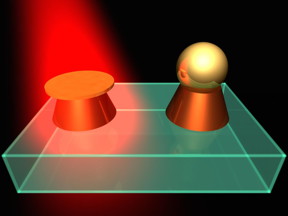 |
| Selective laser exposure to create hybrid nanostructures. CREDIT: ITMO University |
Abstract:
A group of scientists from ITMO University in Saint Petersburg has put forward a new approach to effective manipulation of light at the nanoscale based on hybrid metal-dielectric nanoantennas. The new technology promises to bring about a new platform for ultradense optical data recording and pave the way to high throughput fabrication of a wide range of optical nanodevices capable of localizing, enhancing and manipulating light at the nanoscale. The results of the study were published in Advanced Materials.
Hybrid nanoantennas -- next-generation platform for ultradense data recording
Saint Petersburg, Russia | Posted on April 28th, 2016Nanoantenna is a device that converts freely propagating light into localized light - compressed into several tens of nanometers. The localization enables scientists to effectively control light at the nanoscale. This is one of the reasons why nanoantennas may become the fundamental building blocks of future optical computers that rely on photons instead of electrons to process and transmit information. This inevitable replacement of the information carrier is related to the fact that photons surpass electrons by several orders of magnitude in terms of information capacity, require less energy, rule out circuit heating and ensure high velocity data exchange.
Until recently, the production of planar arrays of hybrid nanoantennas for light manipulation was considered an extremely painstaking process. A solution to this problem was found by researchers from ITMO University in collaboration with colleagues from Saint Petersburg Academic University and Joint Institute for High Temperatures in Moscow. The research group has for the first time developed a technique for creating such arrays of hybrid nanoantennas and for high-accuracy adjustment of individual nanoantennas within the array. The achievement was made possible by subsequently combining two production stages: lithography and precise exposure of thenanoantenna to a femtosecond laser - ultrashort impulse laser.
The practical application of hybrid nanoantennas lies, in particular, within the field of ultradense data recording. Modern optical drives can record information with density around 10 Gbit/inch2, which equals to the size of a single pixel of a few hundred nanometers. Although such dimensions are comparable to the size of the nanoantennas, the scientists propose to additionally control their color in the visible spectrum. This procedure leads to the addition of yet another 'dimension' for data recording, which immediately increases the entire data storage capacity of the system.
Apart from ultradense data recording, the selective modification of hybrid nanoantennas can help create new designs of hybrid metasurfaces, waveguides and compact sensors for environmental monitoring. In the nearest future, the research group plans to focus on the development of such specific applications of their hybrid nanoantennas.
The nanoantennas are made of two components: a truncated silicon cone with a thin golden disk located on top. The researchers demonstrated that, thanks to nanoscale laser reshaping, it is possible to precisely modify the shape of the golden particle without affecting the silicon cone. The change in the shape of the golden particle results in changing optical properties of the nanoantenna as a whole due to different degrees of resonance overlap between the silicon and golden nanoparticles.
"Our method opens a possibility to gradually switch the optical properties of nanoantennas by means of selective laser melting of the golden particles. Depending on the intensity of the laser beam the golden particle will either remain disc-shaped, convert into a cup or become a globe. Such precise manipulation allows us to obtain a functional hybrid nanostructure with desired properties in the flicker of a second," comments Sergey Makarov, one of the authors of the paper and researcher at the Department of Nanophotonics and Metamaterials of ITMO University.
Contrary to conventional heat-induced fabrication of nanoantennas, the new method raises the possibility of adjusting individual nanoantennas within the array and exerting precise control over overall optical properties of the hybrid nanostructures.
"Our concept of asymmetric hybrid nanoantennas unifies two approaches that were previously thought to be mutually exclusive: plasmonics and all-dielectric nanophotonics. Our hybrid nanostructures inherited the advantages of both approaches - localization and enhancement of light at the nanoscale, low optical losses and the ability to control the scattering power pattern. In turn, the use of laser reshaping helps us precisely and quickly change the optical properties of such structures and perhaps even record information with extremely high density," concludes Dmitry Zuev, lead author of the study and researcher at the Department of Nanophotonics and Metamaterials of ITMO University.
####
For more information, please click here
Contacts:
Dmitry Malkov
7-953-377-5508
Copyright © ITMO University
If you have a comment, please Contact us.Issuers of news releases, not 7th Wave, Inc. or Nanotechnology Now, are solely responsible for the accuracy of the content.
Bookmark:


| Related News Press |
News and information
![]() Quantum computer improves AI predictions April 17th, 2026
Quantum computer improves AI predictions April 17th, 2026
![]() Flexible sensor gains sensitivity under pressure April 17th, 2026
Flexible sensor gains sensitivity under pressure April 17th, 2026
![]() A reusable chip for particulate matter sensing April 17th, 2026
A reusable chip for particulate matter sensing April 17th, 2026
![]() Detecting vibrational quantum beating in the predissociation dynamics of SF6 using time-resolved photoelectron spectroscopy April 17th, 2026
Detecting vibrational quantum beating in the predissociation dynamics of SF6 using time-resolved photoelectron spectroscopy April 17th, 2026
Display technology/LEDs/SS Lighting/OLEDs
![]() Spinel-type sulfide semiconductors to operate the next-generation LEDs and solar cells For solar-cell absorbers and green-LED source October 3rd, 2025
Spinel-type sulfide semiconductors to operate the next-generation LEDs and solar cells For solar-cell absorbers and green-LED source October 3rd, 2025
![]() Efficient and stable hybrid perovskite-organic light-emitting diodes with external quantum efficiency exceeding 40 per cent July 5th, 2024
Efficient and stable hybrid perovskite-organic light-emitting diodes with external quantum efficiency exceeding 40 per cent July 5th, 2024
Possible Futures
![]() A fundamentally new therapeutic approach to cystic fibrosis: Nanobody repairs cellular defect April 17th, 2026
A fundamentally new therapeutic approach to cystic fibrosis: Nanobody repairs cellular defect April 17th, 2026
![]() UC Irvine physicists discover method to reverse �quantum scrambling� : The work addresses the problem of information loss in quantum computing system April 17th, 2026
UC Irvine physicists discover method to reverse �quantum scrambling� : The work addresses the problem of information loss in quantum computing system April 17th, 2026
Memory Technology
![]() Researchers tackle the memory bottleneck stalling quantum computing October 3rd, 2025
Researchers tackle the memory bottleneck stalling quantum computing October 3rd, 2025
![]() First real-time observation of two-dimensional melting process: Researchers at Mainz University unveil new insights into magnetic vortex structures August 8th, 2025
First real-time observation of two-dimensional melting process: Researchers at Mainz University unveil new insights into magnetic vortex structures August 8th, 2025
![]() Utilizing palladium for addressing contact issues of buried oxide thin film transistors April 5th, 2024
Utilizing palladium for addressing contact issues of buried oxide thin film transistors April 5th, 2024
Optical computing/Photonic computing
![]() ICFO researchers overcome long-standing bottleneck in single photon detection with twisted 2D materials August 8th, 2025
ICFO researchers overcome long-standing bottleneck in single photon detection with twisted 2D materials August 8th, 2025
![]() Programmable electron-induced color router array May 14th, 2025
Programmable electron-induced color router array May 14th, 2025
Materials/Metamaterials/Magnetoresistance
![]() First real-time observation of two-dimensional melting process: Researchers at Mainz University unveil new insights into magnetic vortex structures August 8th, 2025
First real-time observation of two-dimensional melting process: Researchers at Mainz University unveil new insights into magnetic vortex structures August 8th, 2025
![]() Researchers unveil a groundbreaking clay-based solution to capture carbon dioxide and combat climate change June 6th, 2025
Researchers unveil a groundbreaking clay-based solution to capture carbon dioxide and combat climate change June 6th, 2025
![]() A 1960s idea inspires NBI researchers to study hitherto inaccessible quantum states June 6th, 2025
A 1960s idea inspires NBI researchers to study hitherto inaccessible quantum states June 6th, 2025
![]() Institute for Nanoscience hosts annual proposal planning meeting May 16th, 2025
Institute for Nanoscience hosts annual proposal planning meeting May 16th, 2025
Announcements
![]() A fundamentally new therapeutic approach to cystic fibrosis: Nanobody repairs cellular defect April 17th, 2026
A fundamentally new therapeutic approach to cystic fibrosis: Nanobody repairs cellular defect April 17th, 2026
![]() UC Irvine physicists discover method to reverse �quantum scrambling� : The work addresses the problem of information loss in quantum computing system April 17th, 2026
UC Irvine physicists discover method to reverse �quantum scrambling� : The work addresses the problem of information loss in quantum computing system April 17th, 2026
Interviews/Book Reviews/Essays/Reports/Podcasts/Journals/White papers/Posters
![]() A fundamentally new therapeutic approach to cystic fibrosis: Nanobody repairs cellular defect April 17th, 2026
A fundamentally new therapeutic approach to cystic fibrosis: Nanobody repairs cellular defect April 17th, 2026
![]() UC Irvine physicists discover method to reverse �quantum scrambling� : The work addresses the problem of information loss in quantum computing system April 17th, 2026
UC Irvine physicists discover method to reverse �quantum scrambling� : The work addresses the problem of information loss in quantum computing system April 17th, 2026
Photonics/Optics/Lasers
![]() Metasurfaces smooth light to boost magnetic sensing precision January 30th, 2026
Metasurfaces smooth light to boost magnetic sensing precision January 30th, 2026
![]() From sensors to smart systems: the rise of AI-driven photonic noses January 30th, 2026
From sensors to smart systems: the rise of AI-driven photonic noses January 30th, 2026
|
|
||
|
|
||
| The latest news from around the world, FREE | ||
|
|
||
|
|
||
| Premium Products | ||
|
|
||
|
Only the news you want to read!
Learn More |
||
|
|
||
|
Full-service, expert consulting
Learn More |
||
|
|
||