Home > Press > Penn engineers develop first transistors made entirely of nanocrystal 'inks
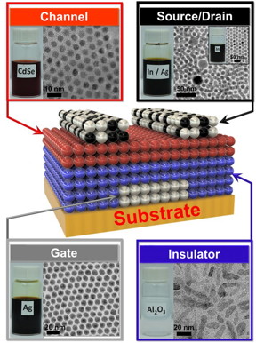 |
| Kagan's group developed a library of four nanocrystal inks that comprise the transistor: a conductor (silver), an insulator (aluminum oxide), a semiconductor (cadmium selenide) and a conductor combined with a dopant (a mixture of silver and indium). Doping the semiconductor layer of the transistor with impurities controls whether the device transmits a positive or negative charge. CREDIT: University of Pennsylvania |
Abstract:
The transistor is the most fundamental building block of electronics, used to build circuits capable of amplifying electrical signals or switching them between the 0s and 1s at the heart of digital computation. Transistor fabrication is a highly complex process, however, requiring high-temperature, high-vacuum equipment.
Penn engineers develop first transistors made entirely of nanocrystal 'inks
Philadelphia, PA | Posted on April 11th, 2016Now, University of Pennsylvania engineers have shown a new approach for making these devices: sequentially depositing their components in the form of liquid nanocrystal "inks."
Their new study, published in Science, opens the door for electrical components to be built into flexible or wearable applications, as the lower-temperature process is compatible with a wide array of materials and can be applied to larger areas.
The researchers' nanocrystal-based field effect transistors were patterned onto flexible plastic backings using spin coating but could eventually be constructed by additive manufacturing systems, like 3-D printers.
The study was lead by Cherie Kagan, the Stephen J. Angello Professor in the School of Engineering and Applied Science, and Ji-Hyuk Choi, then a member of her lab, now a senior researcher at the Korea Institute of Geoscience and Mineral Resources. Han Wang, Soong Ju Oh, Taejong Paik and Pil Sung Jo of the Kagan lab contributed to the work. They collaborated with Christopher Murray, a Penn Integrates Knowledge Professor with appointments in the School of Arts & Sciences and Penn Engineering; Murray lab members Xingchen Ye and Benjamin Diroll; and Jinwoo Sung of Korea's Yonsei University.
The researchers began by taking nanocrystals, or roughly spherical nanoscale particles, with the electrical qualities necessary for a transistor and dispersing these particles in a liquid, making nanocrystal inks.
Kagan's group developed a library of four of these inks: a conductor (silver), an insulator (aluminum oxide), a semiconductor (cadmium selenide) and a conductor combined with a dopant (a mixture of silver and indium). "Doping" the semiconductor layer of the transistor with impurities controls whether the device transmits a positive or negative charge.
"These materials are colloids just like the ink in your inkjet printer," Kagan said, "but you can get all the characteristics that you want and expect from the analogous bulk materials, such as whether they're conductors, semiconductors or insulators.
"Our question was whether you could lay them down on a surface in such a way that they work together to form functional transistors."
The electrical properties of several of these nanocrystal inks had been independently verified, but they had never been combined into full devices.
"This is the first work," Choi said, "showing that all the components, the metallic, insulating, and semiconducting layers of the transistors, and even the doping of the semiconductor could be made from nanocrystals."
Such a process entails layering or mixing them in precise patterns.
First, the conductive silver nanocrystal ink was deposited from liquid on a flexible plastic surface that was treated with a photolithographic mask, then rapidly spun to draw it out in an even layer. The mask was then removed to leave the silver ink in the shape of the transistor's gate electrode. The researchers followed that layer by spin-coating a layer of the aluminum oxide nanocrystal-based insulator, then a layer of the cadmium selenide nanocrystal-based semiconductor and finally another masked layer for the indium/silver mixture, which forms the transistor's source and drain electrodes. Upon heating at relatively low temperatures, the indium dopant diffused from those electrodes into the semiconductor component.
"The trick with working with solution-based materials is making sure that, when you add the second layer, it doesn't wash off the first, and so on," Kagan said. "We had to treat the surfaces of the nanocrystals, both when they're first in solution and after they're deposited, to make sure they have the right electrical properties and that they stick together in the configuration we want."
Because this entirely ink-based fabrication process works at lower temperatures than existing vacuum-based methods, the researchers were able to make several transistors on the same flexible plastic backing at the same time.
"Making transistors over larger areas and at lower temperatures have been goals for an emerging class of technologies, when people think of the Internet of things, large area flexible electronics and wearable devices," Kagan said. "We haven't developed all of the necessary aspects so they could be printed yet, but because these materials are all solution-based, it demonstrates the promise of this materials class and sets the stage for additive manufacturing."
###
The research was supported primarily by the National Science Foundation through its Materials Research Science and Engineering Centers Award DMR-1120901 and its Chemical, Bioengineering, Environmental and Transport Systems Award CBET-1236406; the U.S. Department of Energy, Office of Basic Energy Sciences, Division of Materials Science and Engineering Award DE-SC0002158; and the Office of Naval Research Multidisciplinary University Research Initiative Award ONR-N00014-10-1-0942.
####
For more information, please click here
Contacts:
Evan Lerner
215-573-6604
Copyright © University of Pennsylvania
If you have a comment, please Contact us.Issuers of news releases, not 7th Wave, Inc. or Nanotechnology Now, are solely responsible for the accuracy of the content.
Bookmark:


| Related News Press |
News and information
![]() Quantum computer improves AI predictions April 17th, 2026
Quantum computer improves AI predictions April 17th, 2026
![]() Flexible sensor gains sensitivity under pressure April 17th, 2026
Flexible sensor gains sensitivity under pressure April 17th, 2026
![]() A reusable chip for particulate matter sensing April 17th, 2026
A reusable chip for particulate matter sensing April 17th, 2026
![]() Detecting vibrational quantum beating in the predissociation dynamics of SF6 using time-resolved photoelectron spectroscopy April 17th, 2026
Detecting vibrational quantum beating in the predissociation dynamics of SF6 using time-resolved photoelectron spectroscopy April 17th, 2026
Govt.-Legislation/Regulation/Funding/Policy
![]() Quantum computer improves AI predictions April 17th, 2026
Quantum computer improves AI predictions April 17th, 2026
![]() Metasurfaces smooth light to boost magnetic sensing precision January 30th, 2026
Metasurfaces smooth light to boost magnetic sensing precision January 30th, 2026
![]() New imaging approach transforms study of bacterial biofilms August 8th, 2025
New imaging approach transforms study of bacterial biofilms August 8th, 2025
Possible Futures
![]() A fundamentally new therapeutic approach to cystic fibrosis: Nanobody repairs cellular defect April 17th, 2026
A fundamentally new therapeutic approach to cystic fibrosis: Nanobody repairs cellular defect April 17th, 2026
![]() UC Irvine physicists discover method to reverse �quantum scrambling� : The work addresses the problem of information loss in quantum computing system April 17th, 2026
UC Irvine physicists discover method to reverse �quantum scrambling� : The work addresses the problem of information loss in quantum computing system April 17th, 2026
Chip Technology
![]() A reusable chip for particulate matter sensing April 17th, 2026
A reusable chip for particulate matter sensing April 17th, 2026
![]() Metasurfaces smooth light to boost magnetic sensing precision January 30th, 2026
Metasurfaces smooth light to boost magnetic sensing precision January 30th, 2026
Nanoelectronics
![]() Lab to industry: InSe wafer-scale breakthrough for future electronics August 8th, 2025
Lab to industry: InSe wafer-scale breakthrough for future electronics August 8th, 2025
![]() Interdisciplinary: Rice team tackles the future of semiconductors Multiferroics could be the key to ultralow-energy computing October 6th, 2023
Interdisciplinary: Rice team tackles the future of semiconductors Multiferroics could be the key to ultralow-energy computing October 6th, 2023
![]() Key element for a scalable quantum computer: Physicists from Forschungszentrum J�lich and RWTH Aachen University demonstrate electron transport on a quantum chip September 23rd, 2022
Key element for a scalable quantum computer: Physicists from Forschungszentrum J�lich and RWTH Aachen University demonstrate electron transport on a quantum chip September 23rd, 2022
![]() Reduced power consumption in semiconductor devices September 23rd, 2022
Reduced power consumption in semiconductor devices September 23rd, 2022
Discoveries
![]() Quantum computer improves AI predictions April 17th, 2026
Quantum computer improves AI predictions April 17th, 2026
![]() Flexible sensor gains sensitivity under pressure April 17th, 2026
Flexible sensor gains sensitivity under pressure April 17th, 2026
![]() A reusable chip for particulate matter sensing April 17th, 2026
A reusable chip for particulate matter sensing April 17th, 2026
![]() Detecting vibrational quantum beating in the predissociation dynamics of SF6 using time-resolved photoelectron spectroscopy April 17th, 2026
Detecting vibrational quantum beating in the predissociation dynamics of SF6 using time-resolved photoelectron spectroscopy April 17th, 2026
Materials/Metamaterials/Magnetoresistance
![]() First real-time observation of two-dimensional melting process: Researchers at Mainz University unveil new insights into magnetic vortex structures August 8th, 2025
First real-time observation of two-dimensional melting process: Researchers at Mainz University unveil new insights into magnetic vortex structures August 8th, 2025
![]() Researchers unveil a groundbreaking clay-based solution to capture carbon dioxide and combat climate change June 6th, 2025
Researchers unveil a groundbreaking clay-based solution to capture carbon dioxide and combat climate change June 6th, 2025
![]() A 1960s idea inspires NBI researchers to study hitherto inaccessible quantum states June 6th, 2025
A 1960s idea inspires NBI researchers to study hitherto inaccessible quantum states June 6th, 2025
![]() Institute for Nanoscience hosts annual proposal planning meeting May 16th, 2025
Institute for Nanoscience hosts annual proposal planning meeting May 16th, 2025
Announcements
![]() A fundamentally new therapeutic approach to cystic fibrosis: Nanobody repairs cellular defect April 17th, 2026
A fundamentally new therapeutic approach to cystic fibrosis: Nanobody repairs cellular defect April 17th, 2026
![]() UC Irvine physicists discover method to reverse �quantum scrambling� : The work addresses the problem of information loss in quantum computing system April 17th, 2026
UC Irvine physicists discover method to reverse �quantum scrambling� : The work addresses the problem of information loss in quantum computing system April 17th, 2026
Interviews/Book Reviews/Essays/Reports/Podcasts/Journals/White papers/Posters
![]() A fundamentally new therapeutic approach to cystic fibrosis: Nanobody repairs cellular defect April 17th, 2026
A fundamentally new therapeutic approach to cystic fibrosis: Nanobody repairs cellular defect April 17th, 2026
![]() UC Irvine physicists discover method to reverse �quantum scrambling� : The work addresses the problem of information loss in quantum computing system April 17th, 2026
UC Irvine physicists discover method to reverse �quantum scrambling� : The work addresses the problem of information loss in quantum computing system April 17th, 2026
Military
![]() Quantum engineers �squeeze� laser frequency combs to make more sensitive gas sensors January 17th, 2025
Quantum engineers �squeeze� laser frequency combs to make more sensitive gas sensors January 17th, 2025
![]() Chainmail-like material could be the future of armor: First 2D mechanically interlocked polymer exhibits exceptional flexibility and strength January 17th, 2025
Chainmail-like material could be the future of armor: First 2D mechanically interlocked polymer exhibits exceptional flexibility and strength January 17th, 2025
![]() Single atoms show their true color July 5th, 2024
Single atoms show their true color July 5th, 2024
![]() NRL charters Navy�s quantum inertial navigation path to reduce drift April 5th, 2024
NRL charters Navy�s quantum inertial navigation path to reduce drift April 5th, 2024
Printing/Lithography/Inkjet/Inks/Bio-printing/Dyes
![]() Presenting: Ultrasound-based printing of 3D materials�potentially inside the body December 8th, 2023
Presenting: Ultrasound-based printing of 3D materials�potentially inside the body December 8th, 2023
![]() Simple ballpoint pen can write custom LEDs August 11th, 2023
Simple ballpoint pen can write custom LEDs August 11th, 2023
![]() Disposable electronics on a simple sheet of paper October 7th, 2022
Disposable electronics on a simple sheet of paper October 7th, 2022
|
|
||
|
|
||
| The latest news from around the world, FREE | ||
|
|
||
|
|
||
| Premium Products | ||
|
|
||
|
Only the news you want to read!
Learn More |
||
|
|
||
|
Full-service, expert consulting
Learn More |
||
|
|
||